MC145074D データシートの表示(PDF) - Motorola => Freescale
部品番号
コンポーネント説明
メーカー
MC145074D Datasheet PDF : 14 Pages
| |||
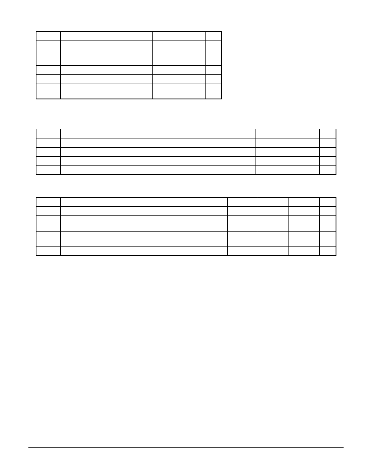
MAXIMUM RATINGS* (Voltages Referenced to VSS)
Symbol
Parameter
Value
Unit
VDD DC Supply Voltage
6.0
V
Vin DC Input Voltage, Any Digital Input
VSS – 0.5 to
V
VDD + 0.5
Iin
DC Input Current, per Pin
Tstg Storage Temperature
TL Lead Temperature, 1 mm from Case for
10 Seconds
±10
mA
– 55 to 150
°C
260
°C
* Maximum Ratings are those values beyond which damage to the device may occur. Func-
tional operation should be restricted to the Operation Ranges below.
This device contains protection circuitry to
guard against damage due to high static volt-
ages or electric fields. However, precautions
must be taken to avoid applications of any volt-
age higher than maximum rated voltages to
this high–impedance circuit. For proper opera-
tion, Vin and Vout should be constrained to the
range VSS ≤ (Vin or Vout) ≤ VDD.
Unused inputs must always be tied to an
appropriate logic voltage level (e.g., either VSS
or VDD). Unused outputs must be left open.
OPERATION RANGES (Applicable to Guaranteed Limits)
Symbol
Parameter
VDD DC Supply Voltage, Referenced to VSS
Vin, Vout Digital Input/Output Voltage
ID
Input Pin Current Drain
TA Operating Temperature
Value
Unit
4.5 to 5.5
V
VSS – 0.5 to VDD + 0.5
V
1
µA
– 40 to + 85
°C
DC ELECTRICAL CHARACTERISTICS
(Voltages Referenced to VSS, Full Temperature and Voltage Ranges per Operation Ranges table, unless otherwise indicated)
Symbol
Parameter
Min
Typ
Max
Unit
Idd Power Supply Current
VIL Input Voltage
VIH
—
—
10
mA
Low Level Input
—
—
VDD x 0.3 V
High Level Input VDD x 0.7
—
—
VOL
VOH
Ilkg
Output Voltage
Input Leakage Current
Low Level Output (Load = 0.4 mA)
—
—
High Level Output (Load = 0.4 mA) VDD – 0.3
—
—
—
0.3
V
—
± 10
µA
MC145074
2
MOTOROLA
Share Link: 