MC145074D データシートの表示(PDF) - Motorola => Freescale
部品番号
コンポーネント説明
メーカー
MC145074D Datasheet PDF : 14 Pages
| |||
DMODE
0
0
0
0
1
1
1
1
RES1
0
0
1
1
0
0
1
1
RES0
0
1
0
1
0
1
0
1
Operating Mode
Dual Data Pin 16–Bit Input
Dual Data Pin 18–Bit Input
Dual Data Pin 20–Bit Input
Factory Test Mode
Single Data Pin 16–Bit Input
Single Data Pin 18–Bit Input
Single Data Pin 20–Bit Input
Factory Test Mode
Figure 8. Serial Interface Formats
FUNCTIONAL DESCRIPTION
The MC145074 is a high precision Stereo Audio Digital–
to–Analog Converter, which utilizes a second–order sigma–
delta modulator with a patented 2–tap architecture that
significantly reduces problems normally associated with
one–bit sigma–delta technology. Normally, a second order
modulator can develop patterns in the digital output repre-
sentation of small signals and with small DC input offsets. It
is common to add dither to mask these effects, but a reduc-
tion of dynamic range can result. The implementation used in
the MC145074 has considerable immunity to these trouble-
some inputs, and without performance compromise.
With RC filtering, the MC145074 can be used as a stand–
alone stereo digital modulator for applications with modest
requirements. High performance can be realized with the
companion MC145076 Stereo Audio FIR Smoothing Filter,
which reduces the in–band IM products formed by large am-
plitude spectral components of the out–of–band noise shap-
ing, clock corruption, and power supply noise.
The MC145074 has been designed for maximum flexibility
and is well suited for high fidelity audio and multimedia
applications. If used in conjunction with a differential
MC145076 smoothing filter, a peak S/(N+D) ratio of > 100 dB
can be achieved by utilizing 18 or 20–bit input data and a
256x oversampling ratio. The MC145074 has a maximum
operating frequency of 18.5 MHz, and can be used with any
sampling rate including 32, 44.1, or 48 kHz.
The MC145074 can accept a 1x, or a 2x input clock with
serial data output chop. The device can accept 16, 18, or
20–bit digital data in a dual data pin input format, or single pin
multiplexed format. An offset scaler is included to allow 0 dB
digital inputs while maintaining low distortion. The offset,
scaled data is applied to the D/A modulator before being op-
tionally chopped (2x mode), and sent to an external smooth-
ing filter. When this device is used with the MC145076,
dividing the clock down or using the chop mode is not neces-
sary.
TIMING CIRCUIT
The internal timing circuits of the MC145074 are driven by
the Xin clock. When the DIV2 pin is active high, the
MC145074 divides the Xin clock by two to generate the in-
ternal modulator clock (MODCLK), and uses the Xin clock
frequency to chop the output data using a 50% chop signal.
When the MC145074 is operated in the master mode, the
WCLK pin is configured as an output. The WCLK output is
generated by dividing down the modulator clock. The divide
MC145074
6
ratio of the internal frequency divider can be programmed
utilizing a 5–bit control word while the MC145074 is in the
standby mode. The 5–bit control word is defined as the last
5–bits (MSB first) that are clocked into the DIR/DILR pin
using the BCLK signal. When cleared, the most significant bit
of the control word indicates that the WCLK signal is nega-
tive edge triggered (just as in the slave mode). If the most
significant bit is set, the WCLK is positive edge triggered.
The next three most significant or middle three bits of the
control word determine the value of the divide ratio of the in-
ternal frequency divider. The least significant bit of the 5–bit
control word indicates a prescaler divide by two when
cleared, and divide by three when set. The divider modes are
summarized in Figure 10.
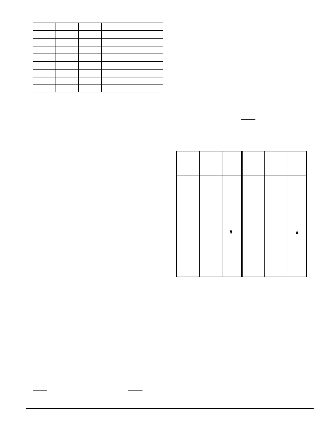
NOTE
The default mode of operation is control word
$06 which provides a WCLK signal (negative
edge triggered) at a frequency of 1/64 the modu-
lator clock frequency. This is the preferred operat-
ing mode of 256x OSR and 4x FIR.
Control
Word
Value
(Hex)
0
1
2
3
4
5
6
7
8
9
A
B
C
D
E
F
Divide
Ratio
8
12
16
24
32
48
64
96
128
192
256
384
512
768
1024
1536
WCLK
Edge
Control
Word
Value
(Hex)
10
11
12
13
14
15
16
17
18
19
1A
1B
1C
1D
1E
1F
Divide
Ratio
8
12
16
24
32
48
64
96
128
192
256
384
512
768
1024
1536
WCLK
Edge
Figure 9. WCLK Divider Modes
OFFSET SCALER
Second order sigma–delta modulators typically give up
about 2 dB of dynamic range and an adjustment to the digital
input words must be made if full scale digital input word
recognition is desired. The offset scaler circuitry of the
MC145074 digitally attenuates the input linearly to 3/4 or
approximately – 2.5 dB. Figure 11 illustrates the function of
the offset scaler block. An ideal DAC would perform as
shown in curve one, but the sigma–delta modulator actually
operates as shown in curve two. The digital input words to
the MC145074 are attenuated to 3/4. This allows the
MC145074 to operate on all 2’s compliment digital inputs
from $80000 to $7FFFF, with the resulting response shown
in curve three. In addition to scaling the digital input word, the
offset scaler adds a digital dc offset of 1/8th to re–center the
digital input word so that the MC145074 output signal is cen-
tered around VDD/2.
MOTOROLA
Share Link: 