AD7450BR гГЗгГЉгВњгВЈгГЉгГИгБЃи°®з§ЇпЉИPDFпЉЙ - Analog Devices
йГ®еУБзХ™еПЈ
гВ≥гГ≥гГЭгГЉгГНгГ≥гГИи™ђжШО
гГ°гГЉгВЂгГЉ
AD7450BR Datasheet PDF : 24 Pages
| |||
PRELIMINARY TECHNICAL DATA
AD7450
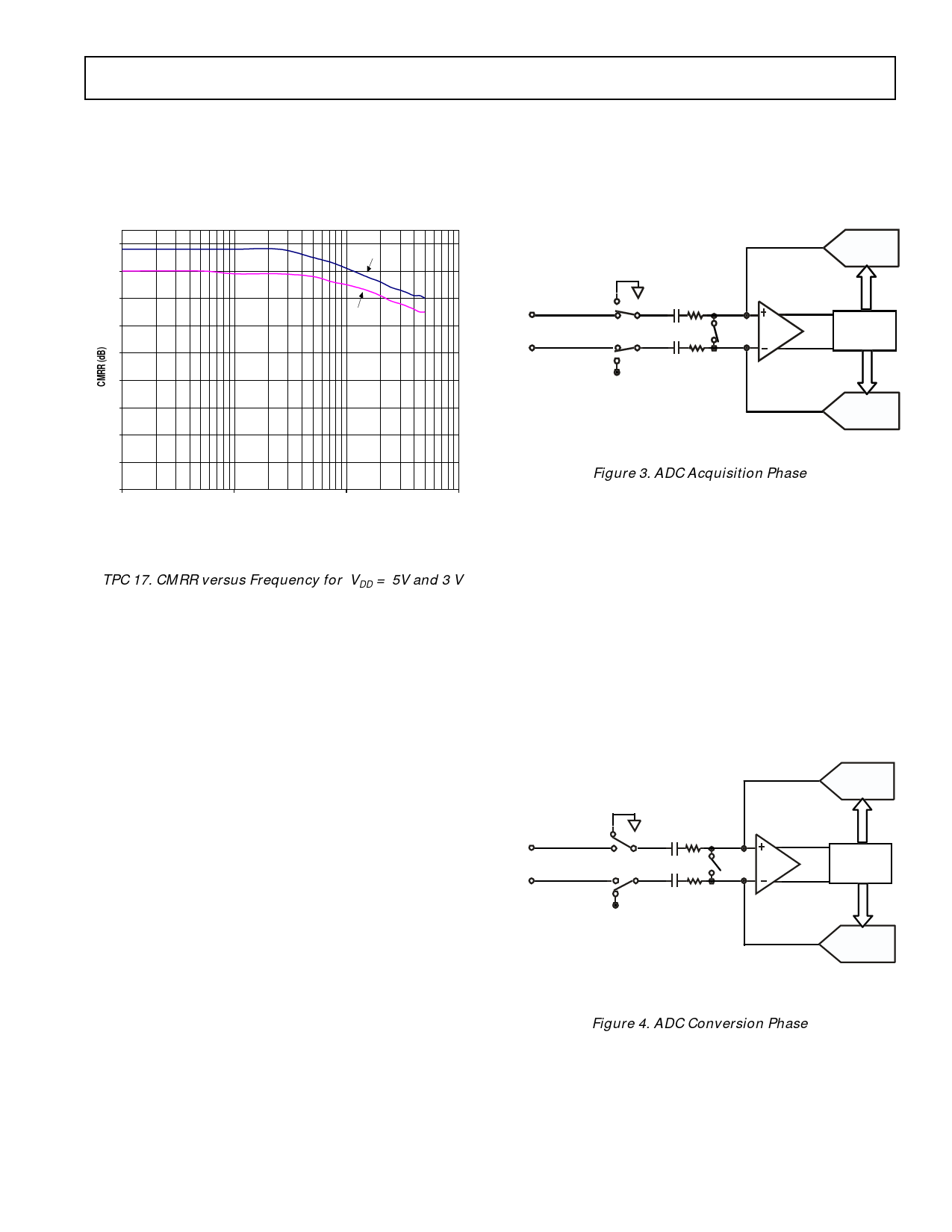
TPC 17 shows the Common Mode Rejection Ratio versus
supply ripple frequency for the AD7450 for both VDD =
5V and 3 V. Here a 200mV p-p sine wave is coupled onto
the Common Mode Voltage of VIN+ and VIN-.
figure 3 (acquisition phase), SW3 is closed and SW1 and
SW2 are in position A, the comparator is held in a bal-
anced condition and the sampling capacitor arrays acquire
the differential signal on the input.
90
VDD = 5 V
80
CAPACITIVE
DAC
70
B
Cs
COMPARATOR
60
50
VDD = 3 V
VIN+
VIN-
A SW1
A SW2
B
Cs
SW3
CONTROL
LOGIC
40
VREF
30
CAPACITIVE
DAC
20
10
0
10
100
1000
10000
Frequency (kHz)
TPC 17. CMRR versus Frequency for VDD = 5V and 3 V
CIRCUIT INFORMATION
The AD7450 is a fast, low power, single supply, 12-bit
successive approximation analog-to-digital converter
(ADC). It can operate with a 5 V and 3V power supply
and is capable of throughput rates up to 1MSPS and
833kSPS when supplied with a 18MHz or 15MHz clock
respectively. This part requires an external reference to be
applied to the VREF pin, with the value of the reference
chosen depending on the power supply and to suit the
application.
When operated with a 5 V supply, the maximum reference
that can be applied to the part is 2.5 V and when operated
with a 3 V supply, the maximum reference that can be
applied to the part is 2.2 V. (See вАШReference SectionвАЩ).
The AD7450 has an on-chip differential track and hold
amplifier, a successive approximation (SAR) ADC and a
serial interface, housed in either an 8-lead SOIC or
µSOIC package. The serial clock input accesses data
from the part and also provides the clock source for the
successive-approximation ADC. The AD7450 features a
power-down option for reduced power consumption be-
tween conversions. The power-down feature is
implemented across the standard serial interface as de-
scribed in the вАШModes of OperationвАЩ section.
CONVERTER OPERATION
The AD7450 is a successive approximation ADC based
around two capacitive DACs. Figures 3 and 4 show sim-
plified schematics of the ADC in Acquisition and
Conversion phase respectively. The ADC comprises of
Control Logic, a SAR and two capacitive DACs. In
Figure 3. ADC Acquisition Phase
When the ADC starts a conversion (figure 4), SW3 will
open and SW1 and SW2 will move to position B, causing
the comparator to become unbalanced. Both inputs are
disconnected once the conversion begins. The Control
Logic and the charge redistribution DACs are used to add
and subtract fixed amounts of charge from the sampling
capacitor arrays to bring the comparator back into a bal-
anced condition. When the comparator is rebalanced, the
conversion is complete. The Control Logic generates the
ADCвАЩs output code. The output impedances of the
sources driving the VIN+ and the VIN- pins must be
matched otherwise the two inputs will have different set-
tling times, resulting in errors.
VIN+
VIN-
B
Cs
A SW1
A SW2
B
VREF
Cs
CAPACITIVE
DAC
COMPARATOR
CONTROL
SW3
LOGIC
CAPACITIVE
DAC
Figure 4. ADC Conversion Phase
ADC TRANSFER FUNCTION
The output coding for the AD7450 is twoвАЩs complement.
The designed code transitions occur at successive LSB
values (i.e. 1LSB, 2LSBs, etc.) and the LSB size is
2xVREF/4096. The ideal transfer characteristic of the
AD7450 is shown in figure 5.
REV. PrJ
вАУ11вАУ
Share Link: 