NE56604-42D データシートの表示(PDF) - Philips Electronics
部品番号
コンポーネント説明
メーカー
NE56604-42D Datasheet PDF : 17 Pages
| |||
Philips Semiconductors
System reset with built-in Watchdog timer
Product data
NE56604-42
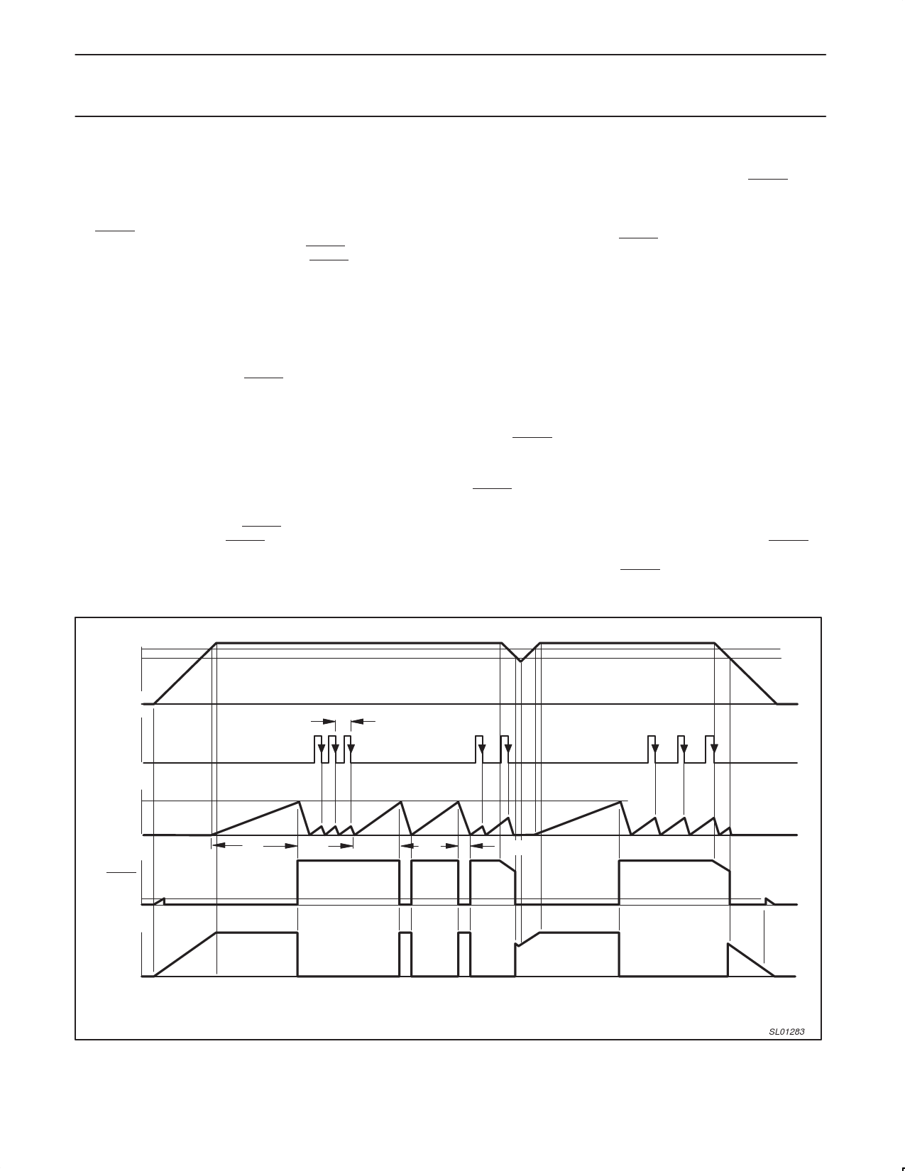
Timing diagram
The timing diagram shown in Figure 20 depicts the operation of the
device. Letters indicate events on the TIME axis.
A: At start-up ‘A’, the VCC and RESET voltages begin to rise. Also
the RESET voltage initially rises, but then abruptly returns to a LOW
state. This is due to VCC reaching the level (RESET 0.8 V) that
activates the internal bias circuitry, asserting RESET.
B: Just before ‘B’, the CT voltage starts to ramp up. This is caused
by, and coincident to, VCC reaching the threshold level of VSH. At
this level the device is in full operation. The RESET output continues
to rise as VCC rises above VSH. This is normal.
C: At ‘C’, VCC is above the undervoltage detect threshold, and CT
has ramped up to its upper detect level. At this point, the device
removes the hold on the resets. RESET goes HIGH while RESET
goes LOW. Also, an internal ramp discharge transistor activates,
discharging CT.
In a microprocessor-based system these events remove the reset
from the microprocessor, allowing it to function normally. The system
must send clock signals to the Watchdog Timer often enough to
prevent CT from ramping up to the CT threshold, to prevent reset
signals from being generated. Each clock signal discharges CT.
C–D: Midway between ‘C’ and ‘D’, the CLK signals cease allowing
the CT voltage to ramp up to its RESET threshold at ‘D’. At this time,
reset signals are generated (RESET goes LOW; RESET goes
HIGH). The device attempts to come out of reset as the CT voltage
is discharged and finally does come out of reset when CLK signals
are re-established after two attempts of CT.
E–F: Immediately before ‘E’, falling VCC causes the RESET signal
to sag. CLK signals are still being received, CT is within normal
operating range, and reset signals are not output. VCC continues to
sag until the VSL undervoltage threshold is reached. At that time,
reset signals are generated (RESET goes LOW; RESET goes
HIGH).
At ‘E’, VCC starts to rise, and the RESET voltage rises with VCC.
However, CT voltage does not start to ramp up until ‘F’, when VCC
reaches the VSH upper threshold.
G: The reset outputs are released at ‘G’ when CT reaches the
upper threshold level again. After ‘G’, normal CLK signals are
received, but at a lower frequency than those following event ‘C’.
The frequency is above the minimum frequency required to keep the
device from outputting reset signals.
G–H: At ‘H’, VCC is normal, CLK signals are being received, and
no reset signals are output. At event ‘H’, the VCC starts falling,
causing RESET to also fall.
J: At event ‘J’, VCC sags to the point where the VSL undervoltage
threshold point is reached, and at that level reset signals are output
(RESET to a LOW state, and RESET to a HIGH state). As the VCC
voltage falls lower, the RESET voltage falls lower.
K: At event ‘K’, the VCC voltage has deteriorated to a level where
normal internal circuit bias is no longer able to maintain a RESET,
and as a result may exhibit a slight rise to something less than 0.8 V.
As VCC decays even further, RESET also decreases to zero.
VSH
VSL
VCC
CLK
CTthresh
CT
RESET
0.8 V
tCLK
tPR
tWDM
tWDR
RESET
A
B
C
D
EF
G
TIME
Figure 20. Timing diagram.
HJ
K
SL01283
2003 Oct 15
10
Share Link: 