AD7834 データシートの表示(PDF) - Analog Devices
部品番号
コンポーネント説明
メーカー
AD7834 Datasheet PDF : 28 Pages
| |||
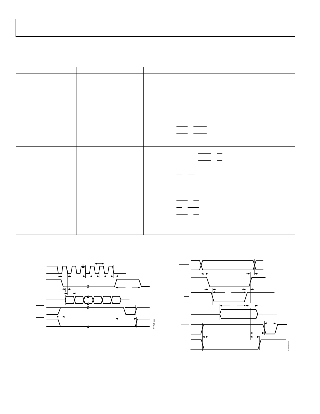
AD7834/AD7835
TIMING SPECIFICATIONS
VCC = 5 V ± 5%; VDD = 11.4 V to 15.75 V; VSS = −11.4 V to −15.75 V; AGND = DGND = 0 V1.
Table 4.
Parameter
AD7834-SPECIFIC
t1 2
t22
t32
t4
t5
t6
t7
t8
t9
t21
AD7835-SPECIFIC
t11
t12
t13
t14
t15
t16
t17
t18
t19
t20
GENERAL
t10
Limit at TMIN, TMAX
100
50
30
30
40
30
10
0
40
20
15
15
0
0
40
40
10
0
0
0
40
Unit
ns min
ns min
ns min
ns min
ns min
ns min
ns min
ns min
ns min
ns min
ns min
ns min
ns min
ns min
ns min
ns min
ns min
ns min
ns min
ns min
ns min
Description
SCLK cycle time
SCLK low
SCLK high time
FSYNC, PAEN setup time
FSYNC, PAEN hold time
Data setup time
Data hold time
LDAC to FSYNC setup time
LDAC to FSYNC hold time
Delay between write operations
A0, A1, A2, BYSHF to CS setup time
A0, A1, A2, BYSHF to CS hold time
CS to WR setup time
CS to WR hold time
WR pulse width
Data setup time
Data hold time
LDAC to CS setup time
CS to LDAC setup time
LDAC to CS hold time
LDAC, CLR pulse width
1 All input signals are specified with tr = tf = 5 ns (10% to 90% of 5 V) and time from a voltage level of 1.6 V.
2 Rise and fall times should be no longer than 50 ns.
SCLK
FSYNC
DIN
LDAC
(SIMULTANEOUS
UPDATE)
LDAC
(PER-CHANNE L
UPDATE)
1ST 2ND
CLK CLK
t1
24TH
CLK
t4
t2
MSB
t6
t7
D23 D22
t8
t3
t5
t 21
LSB
D1 D0
t 10
t9
Figure 3. AD7834 Timing Diagram
A0 A1 A2
BYSHF
CS
WR
DB0 TO DB13
LDAC
(SIMULTANEOUS
UPDATE)
LDAC
(PER-CHANNEL
UPDATE)
t 11
t13
t15
t16
t 12
t 14
t17
t10
t19
t 18
t20
Figure 4. AD7835 Timing Diagram
Rev. D | Page 6 of 28
Share Link: 