AD7834 データシートの表示(PDF) - Analog Devices
部品番号
コンポーネント説明
メーカー
AD7834 Datasheet PDF : 28 Pages
| |||
AD7834/AD7835
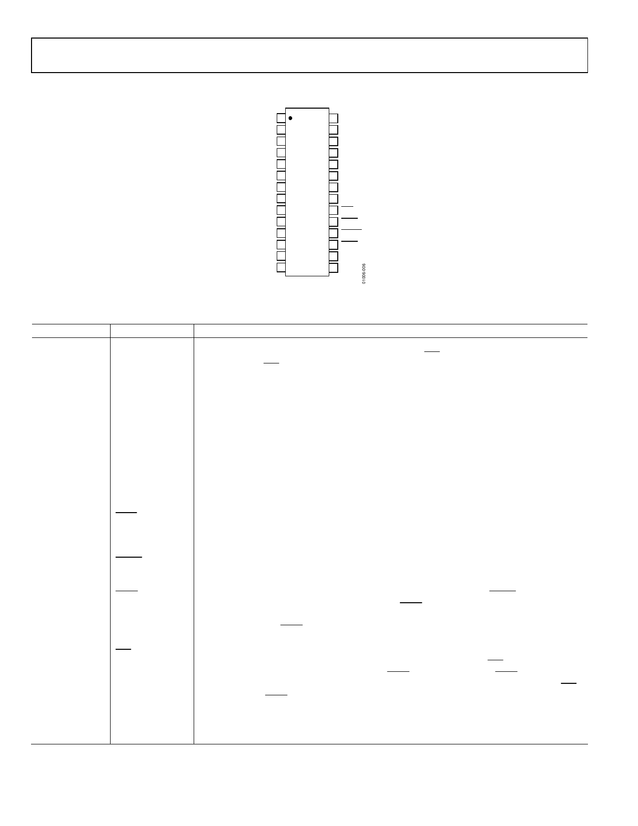
PIN CONFIGURATIONS AND FUNCTION DESCRIPTIONS
VSS 1
DSG 2
28 AGND
27 NC
VREF(–) 3
26 NC
VREF(+) 4
25 NC
NC 5 AD7834 24 NC
VOUT2 6 TOP VIEW 23 VDD
VOUT4 7 (Not to Scale) 22 VOUT1
DGND 8
VCC 9
21 VOUT3
20 CLR
SCLK 10
19 LDAC
DIN 11
18 FSYNC
PA0 12
17 PAEN
PA1 13
16 PA4
PA2 14
15 PA3
NC = NO CONNECT
Figure 6. AD7834 PDIP and SOIC Pin Configuration
Table 7. AD7834 Pin Function Descriptions
Pin No.
Pin Mnemonic Description
1
VSS
Negative Analog Power Supply: −15 V ± 5% or −12 V ± 5%.
2
DSG
Device Sense Ground Input. Used in conjunction with the CLR input for power-on protection of
the DACs. When CLR is low, the DAC outputs are forced to the potential on the DSG pin.
3
4
5, 24, 25, 26, 27
VREF(−)
VREF(+)
NC
Negative Reference Input. The negative reference voltage is referred to AGND.
Positive Reference Input. The positive reference voltage is referred to AGND.
No Connect.
22, 6, 21, 7
8
VOUT1 to VOUT4
DGND
DAC Outputs.
Digital Ground.
9
VCC
Logic Power Supply: 5 V ± 5%.
10
SCLK
Clock Input. Used for writing data to the device; data is clocked into the input register on the
falling edge of SCLK.
11
DIN
Serial Data Input.
12,13,14,15,16 PA0 to PA4
Package Address Inputs. These inputs are hardwired high (VCC) or low (DGND) to assign dedicated
package addresses in a multipackage environment.
17
PAEN
Package Address Enable Input. When low, this input allows normal operation of the device. When
high, the device ignores the package address, but not the channel address, in the serial data
stream and loads the serial data into the input registers. This feature is useful in a multipackage
application where it can be used to load the same data into the same channel in each package.
18
FSYNC
Frame Sync Input. Active low logic input used, in conjunction with DIN and SCLK, to write data to
the device with serial data expected after the falling edge of this signal. The contents of the 24-bit
serial-to-parallel input register are transferred on the rising edge of this signal.
19
LDAC
Load DAC Input (Level Sensitive). This input signal, in conjunction with the FSYNC input signal,
determines how the analog outputs are updated. If LDAC is maintained high while new data is
being loaded into the device’s input registers, no change occurs on the analog outputs.
Subsequently, when LDAC is brought low, the contents of all four input registers are transferred
into their respective DAC latches, updating all of the analog outputs simultaneously.
20
CLR
Asynchronous Clear Input (Level Sensitive, Active Low). When this input is brought low, all analog
outputs are switched to the externally set potential on the DSG pin. When CLR is brought high, the
signal outputs remain at the DSG potential until LDAC is brought low. When LDAC is brought low,
the analog outputs are switched back to reflect their individual DAC output levels. As long as CLR
remains low, the LDAC signals are ignored, and the signal outputs remain switched to the
potential on the DSG pin.
23
VDD
Positive Analog Power Supply: 15 V ± 5% or 12 V ± 5%.
28
AGND
Analog Ground.
Rev. D | Page 8 of 28
Share Link: 