TEA0676T データシートの表示(PDF) - Philips Electronics
部品番号
コンポーネント説明
メーカー
TEA0676T Datasheet PDF : 20 Pages
| |||
Philips Semiconductors
Dual pre-amplifier and equalizer for
reverse tape decks
Product specification
TEA0676T
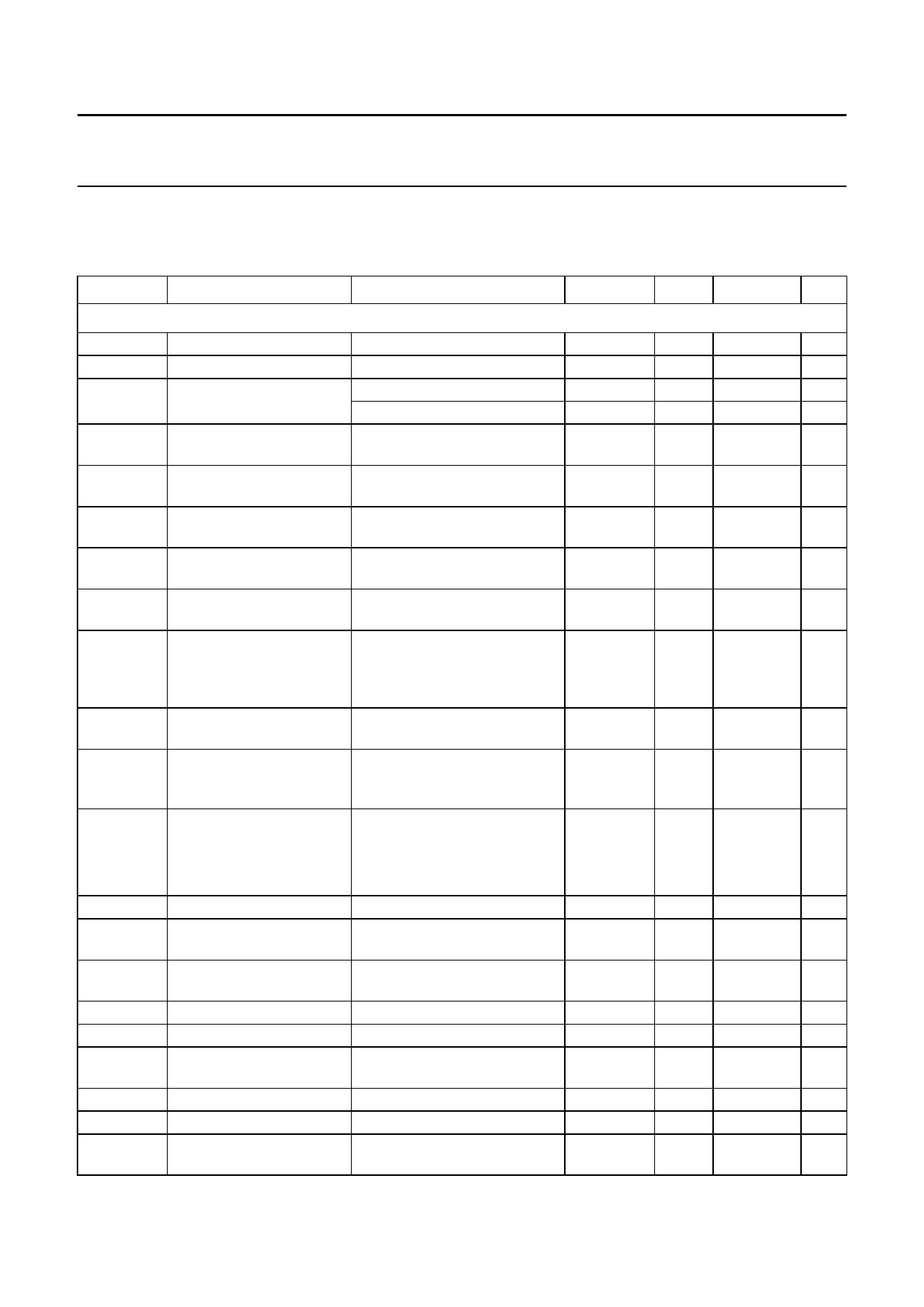
CHARACTERISTICS
VCC = 10 V; RL = 10 kΩ; CL = 2.5 nF; Tamb = 25 °C; Vo = 0 dB means 387.5 mV at output; all levels are referenced to
387.5 mV with 0 dB as standard; EQ switch in 70 µs position; unless otherwise specified; see notes 1 and 2.
SYMBOL
PARAMETER
CONDITIONS
MIN.
TYP.
MAX. UNIT
Supply
VCC
supply voltage (pin 5)
7.6
ICC
supply current
−
THD
total harmonic distortion f = 1 kHz; Vo = 0 dB
−
f = 10 kHz; Vo = 6 dB
−
HR
headroom at output
VCC = 7.6 V; THD = 1%;
12
f = 1 kHz
10.0 12.0
V
10
13
mA
0.08 0.15
%
0.15 0.3
%
−
−
dB
PSRR
power supply ripple
VR(rms) < 0.25 V; f = 1 kHz
−
50
−
dB
rejection
αcs
channel separation
selective measurement;
57
63
−
dB
f = 1 kHz; Vo = 10 dB
αm
channel matching
selective measurement;
−0.5
−
+0.5
dB
f = 1 kHz; Vo = 0 dB
αct
crosstalk between active selective measurement;
70
77
−
dB
and inactive input
f = 1 kHz; Vo = 10 dB
S------N+-----N---
signal plus noise-to-noise unweighted;
67
ratio (RMS value)
f = 20 Hz to 20 kHz; Rs = 0 Ω;
73
−
dB
internal gain 40 dB; linear;
see Fig.13
Vno(rms)
equivalent input noise
unweighted;
−
0.8
−
µV
voltage (RMS value)
f = 20 Hz to 20 kHz; Rs = 0 Ω
Gv
voltage gain of
pre-amplifier
from pin INA1 or INA2 to
29
30
31
dB
pin EQINA and from pin INB1
or INB2 to pin EQINB
Av
open-loop amplification pin INA1 to pin OUTA and
pin INB1 to pin OUTB
REQ
equalization resistor
ZI
input impedance
pre-amplifier
f = 10 kHz
f = 400 Hz
80
86
−
dB
104
110 −
dB
4.7
5.8
6.9
kΩ
60
100 −
kΩ
ZO
output impedance
EQ-amplifier
−
80
100
Ω
RL
output load resistance
10
−
−
kΩ
CL
output load capacitance
0
−
10
nF
Voffset(DC) input offset voltage
pins INA1, INA2, INB1 and
−
2
−
mV
INB2 connected to Vref
IO(GND)
DC current capability
output to ground
−2
−
−
mA
IO(VCC)
DC current capability
output to VCC
300
−
−
µA
EMC
DC offset voltage at
f = 900 MHz; Vi = 6 V (RMS); −
50
−
mV
pins 1 and 16
see Figs 12, 14 and 15
1997 Oct 07
6
Share Link: 