MC14060BD データシートの表示(PDF) - Motorola => Freescale
部品番号
コンポーネント説明
メーカー
MC14060BD Datasheet PDF : 6 Pages
| |||
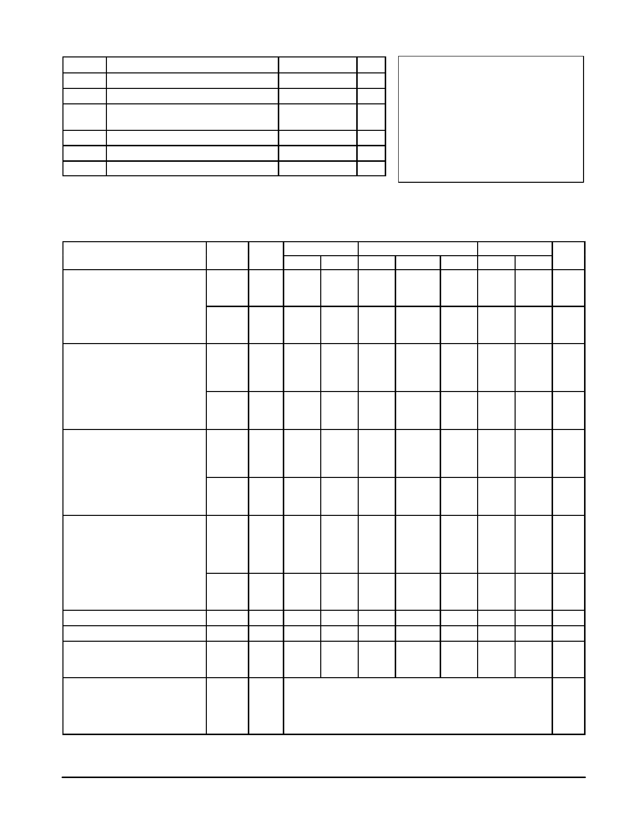
ÎÎÎÎÎÎÎÎÎÎÎÎÎÎÎÎÎÎÎÎÎÎÎÎÎÎÎÎÎÎÎÎÎÎÎÎÎÎÎÎÎÎÎÎÎÎÎÎÎÎÎÎÎÎÎÎÎÎÎÎÎÎÎÎÎÎ MAXIMUM RATINGS* (Voltages Referenced to VSS)
ÎÎÎÎÎÎÎÎÎÎÎÎÎÎÎÎÎÎÎÎÎÎ Symbol
Parameter
Value
Unit
ÎÎÎÎÎÎÎÎÎÎÎÎÎÎÎÎÎÎÎÎÎÎ VDD
ÎÎÎÎÎÎÎÎÎÎÎÎÎÎÎÎÎÎÎÎÎÎ Vin, Vout
ÎÎÎÎÎÎÎÎÎÎÎÎÎÎÎÎÎÎÎÎÎÎ Iin, Iout
DC Supply Voltage
Input or Output Voltage (DC or Transient)
Input or Output Current (DC or Transient),
per Pin
– 0.5 to + 18.0
V
– 0.5 to VDD + 0.5 V
± 10
mA
ÎÎÎÎÎÎÎÎÎÎÎÎÎÎÎÎÎÎÎÎÎÎÎÎÎÎÎÎÎÎÎÎÎÎÎÎÎÎÎÎÎÎÎÎ PD
Power Dissipation, per Package†
500
mW
Tstg Storage Temperature
– 65 to + 150
_C
ÎÎÎÎÎÎÎÎÎÎÎÎÎÎÎÎÎÎÎÎÎÎ TL
Lead Temperature (8–Second Soldering)
260
_C
ÎÎÎÎÎÎÎÎÎÎÎÎÎÎÎÎÎÎÎÎÎÎ * Maximum Ratings are those values beyond which damage to the device may occur.
ÎÎÎÎÎÎÎÎÎÎÎÎÎÎÎÎÎÎÎÎÎÎÎÎÎÎÎÎÎÎÎÎÎÎ †Temperature Derating:
Plastic “P and D/DW” Packages: – 7.0 mW/_C From 65_C To 125_C
ÎÎÎÎÎÎÎÎÎÎÎÎÎÎÎÎÎÎÎÎÎÎÎÎÎÎÎÎÎÎÎÎÎÎ Ceramic “L” Packages – 12 mW/_C From 100_C To 125_C
This device contains protection circuitry to
guard against damage due to high static
voltages or electric fields. However, pre-
cautions must be taken to avoid applications of
any voltage higher than maximum rated volt-
ages to this high–impedance circuit. For proper
v v operation, Vin and Vout should be constrained
to the range VSS (Vin or Vout) VDD.
Unused inputs must always be tied to an
appropriate logic voltage level (e.g., either VSS
or VDD). Unused outputs must be left open.
ÎÎÎÎÎÎÎÎÎÎÎÎÎÎÎÎÎÎÎÎÎÎÎÎÎÎÎÎÎÎÎÎÎÎÎÎÎÎÎÎÎÎÎÎÎÎÎÎÎÎÎÎÎÎÎÎÎÎÎÎÎÎÎÎÎÎÎÎ ELECTRICAL CHARACTERISTICS (Voltages Referenced to VSS)
ÎÎÎÎÎÎÎÎÎÎÎÎÎÎÎÎÎÎÎÎÎÎÎÎÎÎÎÎÎÎÎÎÎÎ Characteristic
VDD
– 55_C
25_C
125_C
Symbol Vdc
Min
Max
Min
Typ #
Max
Min
Max Unit
ÎÎÎÎÎÎÎÎÎÎÎÎÎÎÎÎÎÎÎÎÎÎÎÎÎÎÎÎÎÎÎÎÎÎ Output Voltage
ÎÎÎÎÎÎÎÎÎÎÎÎÎÎÎÎÎÎÎÎÎÎÎÎÎÎÎÎÎÎÎÎÎÎ Vin = VDD or 0
“0” Level VOL
5.0
—
0.05
—
10
—
0.05
—
15
—
0.05
—
0
0.05
—
0.05
V
0
0.05
—
0.05
0
0.05
—
0.05
ÎÎÎÎÎÎÎÎÎÎÎÎÎÎÎÎÎÎÎÎÎÎÎÎÎÎÎÎÎÎÎÎÎÎÎÎÎÎÎÎÎÎÎÎÎÎÎÎÎÎÎÎÎÎÎÎÎÎÎÎÎÎÎÎÎÎÎÎÎÎÎÎÎÎÎÎÎÎÎÎÎÎÎÎÎÎÎÎÎÎÎÎÎÎÎÎÎÎÎÎÎÎ Vin = 0 or VDD
“1” Level VOH
5.0
4.95
—
4.95
5.0
10
9.95
—
9.95
10
15
14.95
—
14.95
15
—
4.95
—
V
—
9.95
—
—
14.95
—
ÎÎÎÎÎÎÎÎÎÎÎÎÎÎÎÎÎÎÎÎÎÎÎÎÎÎÎÎÎÎÎÎÎÎ Input Voltage
“0” Level VIL
V
ÎÎÎÎÎÎÎÎÎÎÎÎÎÎÎÎÎÎÎÎÎÎÎÎÎÎÎÎÎÎÎÎÎÎ (VO = 4.5 or 0.5 V)
5.0
—
1.5
—
2.25
1.5
—
1.5
(VO = 9.0 or 1.0 V)
10
—
3.0
—
4.50
3.0
—
3.0
ÎÎÎÎÎÎÎÎÎÎÎÎÎÎÎÎÎÎÎÎÎÎÎÎÎÎÎÎÎÎÎÎÎÎ (VO = 13.5 or 1.5 V)
15
—
4.0
—
6.75
4.0
—
4.0
ÎÎÎÎÎÎÎÎÎÎÎÎÎÎÎÎÎÎÎÎÎÎÎÎÎÎÎÎÎÎÎÎÎÎ (VO = 0.5 or 4.5 V) “1” Level VIH
5.0
3.5
—
3.5
2.75
—
3.5
—
V
(VO = 1.0 or 9.0 V)
10
7.0
—
7.0
5.50
—
7.0
—
ÎÎÎÎÎÎÎÎÎÎÎÎÎÎÎÎÎÎÎÎÎÎÎÎÎÎÎÎÎÎÎÎÎÎ (VO = 1.5 or 13.5 V)
15
11.0
—
11.0
8.25
—
11.0
—
ÎÎÎÎÎÎÎÎÎÎÎÎÎÎÎÎÎÎÎÎÎÎÎÎÎÎÎÎÎÎÎÎÎÎ Input Voltage
“0” Level VIL
Vdc
ÎÎÎÎÎÎÎÎÎÎÎÎÎÎÎÎÎÎÎÎÎÎÎÎÎÎÎÎÎÎÎÎÎÎ (VO = 4.5 Vdc) (For Input 11
5.0
—
1.0
—
2.25
1.0
—
1.0
ÎÎÎÎÎÎÎÎÎÎÎÎÎÎÎÎÎÎÎÎÎÎÎÎÎÎÎÎÎÎÎÎÎÎ (VO = 9.0 Vdc) and Output 10)
10
—
2.0
—
4.50
2.0
—
2.0
(VO = 13.5 Vdc)
15
—
2.5
—
6.75
2.5
—
2.5
ÎÎÎÎÎÎÎÎÎÎÎÎÎÎÎÎÎÎÎÎÎÎÎÎÎÎÎÎÎÎÎÎÎÎ (VO = 0.5 Vdc)
ÎÎÎÎÎÎÎÎÎÎÎÎÎÎÎÎÎÎÎÎÎÎÎÎÎÎÎÎÎÎÎÎÎÎ (VO = 1.0 Vdc)
ÎÎÎÎÎÎÎÎÎÎÎÎÎÎÎÎÎÎÎÎÎÎÎÎÎÎÎÎÎÎÎÎÎÎ (VO = 1.5 Vdc)
“1” Level VIH
5.0
4.0
—
4.0
2.75
10
8.0
—
8.0
5.50
15
12.5
—
12.5
8.25
—
4.0
—
Vdc
—
8.0
—
—
12.5
—
ÎÎÎÎÎÎÎÎÎÎÎÎÎÎÎÎÎÎÎÎÎÎÎÎÎÎÎÎÎÎÎÎÎÎ Output Drive Current
IOH
mA
(VOH = 2.5 V) (Except Source
5.0 – 3.0
—
– 2.4
– 4.2
—
– 1.7
—
ÎÎÎÎÎÎÎÎÎÎÎÎÎÎÎÎÎÎÎÎÎÎÎÎÎÎÎÎÎÎÎÎÎÎ (VOH = 4.6 V) Pins 9 and 10)
5.0 – 0.64
—
– 0.51 – 0.88
—
– 0.36
—
ÎÎÎÎÎÎÎÎÎÎÎÎÎÎÎÎÎÎÎÎÎÎÎÎÎÎÎÎÎÎÎÎÎÎ (VOH = 9.5 V)
10
– 1.6
—
– 1.3 – 2.25
—
– 0.9
—
(VOH = 13.5 V)
15
– 4.2
—
– 3.4
– 8.8
—
– 2.4
—
ÎÎÎÎÎÎÎÎÎÎÎÎÎÎÎÎÎÎÎÎÎÎÎÎÎÎÎÎÎÎÎÎÎÎ (VOL = 0.4 V)
ÎÎÎÎÎÎÎÎÎÎÎÎÎÎÎÎÎÎÎÎÎÎÎÎÎÎÎÎÎÎÎÎÎÎ (VOL = 0.5 V)
ÎÎÎÎÎÎÎÎÎÎÎÎÎÎÎÎÎÎÎÎÎÎÎÎÎÎÎÎÎÎÎÎÎÎ (VOL = 1.5 V)
Sink IOL
ÎÎÎÎÎÎÎÎÎÎÎÎÎÎÎÎÎÎÎÎÎÎÎÎÎÎÎÎÎÎÎÎÎÎ Input Current
Iin
ÎÎÎÎÎÎÎÎÎÎÎÎÎÎÎÎÎÎÎÎÎÎÎÎÎÎÎÎÎÎÎÎÎÎ Input Capacitance (Vin = 0)
Cin
Quiescent Current
IDD
ÎÎÎÎÎÎÎÎÎÎÎÎÎÎÎÎÎÎÎÎÎÎÎÎÎÎÎÎÎÎÎÎÎÎÎÎÎÎÎÎÎÎÎÎÎÎÎÎÎÎÎÎÎÎÎÎÎÎÎÎÎÎÎÎÎÎÎÎ (Per Package)
5.0
0.64
—
0.51
0.88
10
1.6
—
1.3
2.25
15
4.2
—
3.4
8.8
—
0.36
—
mA
—
0.9
—
—
2.4
—
15
—
± 0.1
— ± 0.00001 ± 0.1
—
± 1.0 µA
—
—
—
—
5.0
7.5
—
—
pF
5.0
—
5.0
—
0.005
5.0
—
150
µA
10
—
10
—
0.010
10
—
300
15
—
20
—
0.015
20
—
600
ÎÎÎÎÎÎÎÎÎÎÎÎÎÎÎÎÎÎÎÎÎÎÎÎÎÎÎÎÎÎÎÎÎÎ Total Supply Current**†
IT
5.0
IT = (0.25 µA/kHz) f + IDD
µA
(Dynamic plus Quiescent,
10
IT = (0.54 µA/kHz) f + IDD
ÎÎÎÎÎÎÎÎÎÎÎÎÎÎÎÎÎÎÎÎÎÎÎÎÎÎÎÎÎÎÎÎÎÎ Per Package)
15
IT = (0.85 µA/kHz) f + IDD
ÎÎÎÎÎÎÎÎÎÎÎÎÎÎÎÎÎÎÎÎÎÎÎÎÎÎÎÎÎÎÎÎÎÎ (CL = 50 pF on all outputs,
ÎÎÎÎÎÎÎÎÎÎÎÎÎÎÎÎÎÎÎÎÎÎÎÎÎÎÎÎÎÎÎÎÎÎ all buffers switching)
# Data labelled “Typ” is not to be used for design purposes but is intended as an indication of the IC’s potential performance.
** The formulas given are for the typical characteristics only at 25_C.
MC14060B
2
MOTOROLA CMOS LOGIC DATA
Share Link: 