LR38574 データシートの表示(PDF) - Sharp Electronics
部品番号
コンポーネント説明
メーカー
LR38574 Datasheet PDF : 9 Pages
| |||
LR38574
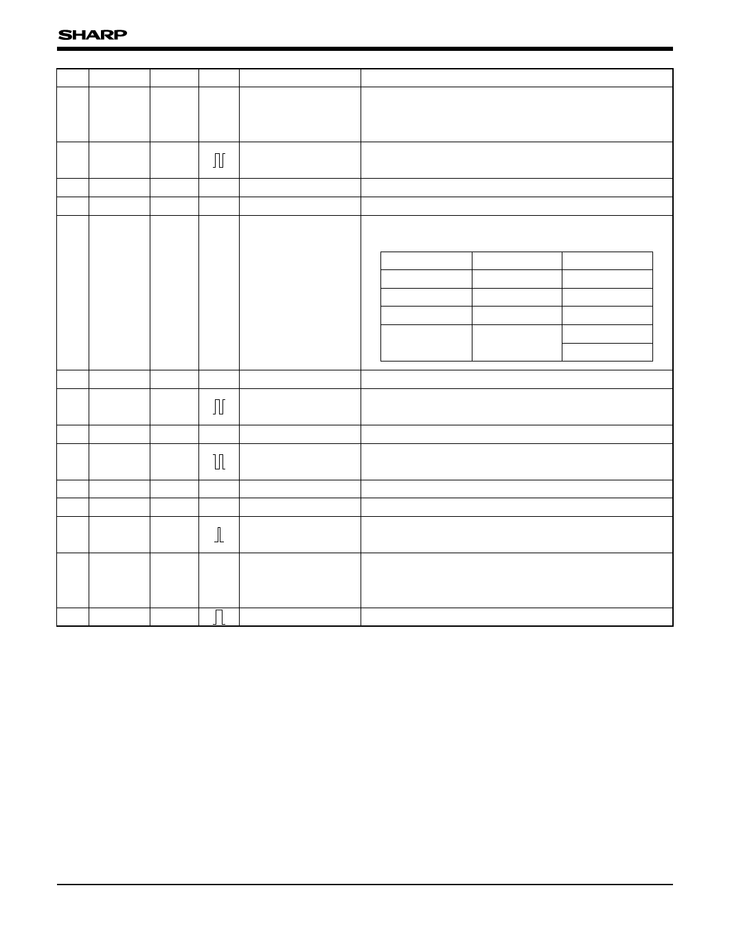
PIN NO. SYMBOL I/O POLARITY
PIN NAME
35 ED2
ICSU3
Shift register data
–
input
36 ID
37 TST1
38 TST2
O3
ICD4
ICD4
Line index pulse
output
– Test pin 1
– Test pin 2
39 CCD
ICU4 – CCD selection input
DESCRIPTION
An input pin for the data of the shift register, to control
the functions of LR38574. For details, see "Serial Data
Control".
The pulse is used in color separator.
The signal switches between high and low at every line.
A test pin. Set open or to L level in the normal mode.
A test pin. Set open or to L level in the normal mode.
An input pin to select CCD. It should be used with
MODE input which is in the serial data.
CCD
MODE
CCD
L
L
LZ23H3V1
L
H
–
H
L
LZ23J3V
–
H
H
–
40 VDD4
–
– Power supply
Supply of +4.5 V power.
41 FH1
O6MA43
Horizontal transfer
pulse output 1
A horizontal transfer pulse for CCD.
Connect to ØH1 pin of CCD.
42 GND
–
– Ground
A grounding pin.
43 FH2
44 VDD4
O6MA43
–
–
Horizontal transfer
pulse output 2
Power supply
A horizontal transfer pulse for CCD.
Connect to ØH2 pin of CCD.
Supply of +4.5 V power.
45 TST3
46 FR
ICD4 –
O6MA43
Test pin 3
Reset pulse output
A test pin. Set open or to L level in the normal mode.
A pulse to reset the charge of output circuit.
The output phase of FR is selected by serial data.
47 DRMD
ICU3
An input pin to select the period of still mode.
Drive mode selection
–
L level
: 3 fields period
input
H level or open : 4 fields period
48 SHTR
O3
Trigger output
A trigger pulse for effective signal period.
IC3
ICU3
ICSU3
ICU4
ICD4
: Input pin (CMOS level)
: Input pin (CMOS level with pull-up resistor)
: Input pin (CMOS level with schmitt-trigger)
: Input pin (CMOS level with pull-up resistor)
: Input pin (CMOS level with pull-down resistor)
O3
: Output pin (output high level is VDD3.)
O6MA3 : Output pin (output high level is VDD3.)
O6MA43 : Output pin (output high level is VDD4.)
OSCI3 : Input pin for oscillation
OSCO3 : Output pin for oscillation
5
Share Link: 