LR38581 データシートの表示(PDF) - Sharp Electronics
部品番号
コンポーネント説明
メーカー
LR38581
Sharp Electronics

LR38581 Datasheet PDF : 8 Pages
| |||
LR38581
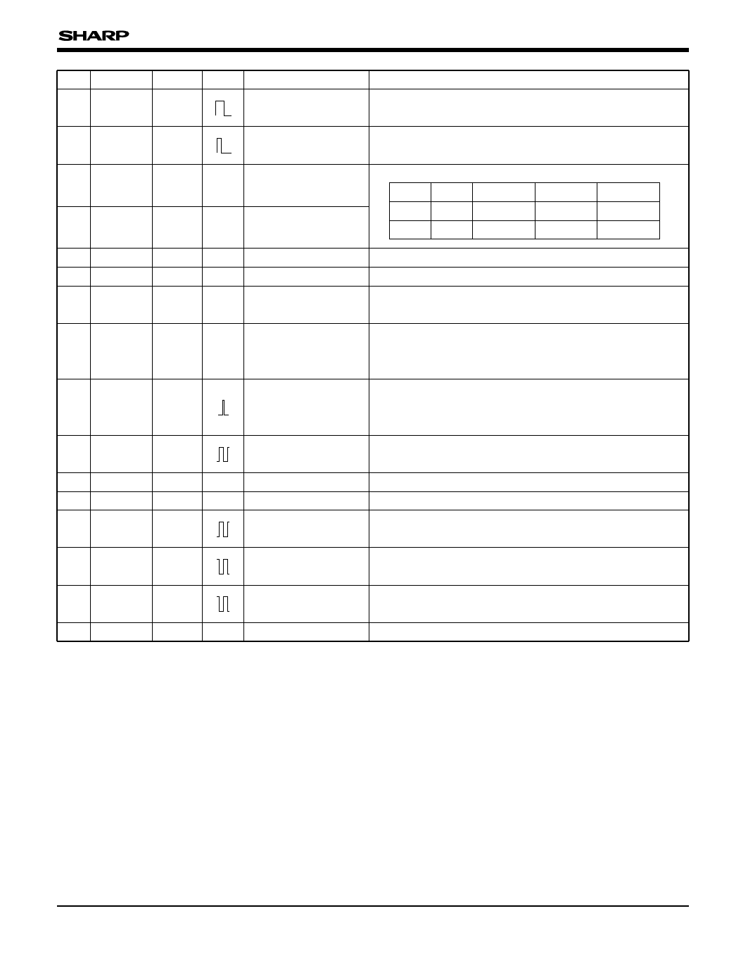
PIN NO. SYMBOL
33 VD
I/O POLARITY
PIN NAME
Vertical reference
IC3
pulse input
DESCRIPTION
An input pin for reference of vertical pulse.
Connect to VD pin of DSP IC.
34 HP
IC3
Horizontal reference An input pin for reference of horizontal pulse.
pulse input
Connect to HD pin of DSP IC.
35 SAD1
36 SAD2
ICU3
ICU3
ADCK phase control An input pin to select the phase of ADCK.
–
input 1
SAD1 L H or open
L
H or open
ADCK phase control
–
input 2
SAD2 L
L
H or open H or open
Phase 0˚ 60˚ delay 180˚ delay 240˚ delay
37 TST3
ICD5 – Test pin 3
A test pin. Set open or to L level in the normal mode.
38 TST4
39 PLCH
ICD5
ICU5
– Test pin 4
Polarity selection
–
input
A test pin. Set open or to L level in the normal mode.
An input pin to select the polarity of OBCP (pin 1),
CLP (pin 2), FS (pin 4), FCDS (pin 5) and RS (pin 6).
40 TVMD
ICU5
An input pin to select TV standards.
TV mode selection
–
L level
: NTSC mode
input
H level or open : PAL mode
A pulse to reset the charge of output circuit.
41 FR
O4MA53
Reset pulse output Connect to ØR pin of CCD through the DC offset circuit.
The output phase of FR is selected by serial data.
42 FH1B O4MA52
Horizontal transfer
pulse output 1B
A pulse to drive horizontal CCD shift register.
Connect to ØH1B pin of CCD.
43 GND
–
– Ground
A grounding pin.
44 VDD5
–
– Power supply
Supply of +5 V power.
45 FH1
O4MA53
Horizontal transfer
pulse output 1
A pulse to drive horizontal CCD shift register.
Connect to ØH1 pin of CCD.
46 FH2
O4MA53
Horizontal transfer
pulse output 2
A pulse to drive horizontal CCD shift register.
Connect to ØH2 pin of CCD.
47 FH2B O4MA52
Horizontal transfer
pulse output 2B
A pulse to drive horizontal CCD shift register.
Connect to ØH2B pin of CCD.
48 GND
–
– Ground
A grounding pin.
IC3
ICU3
ICSU3
ICU5
ICD5
O4MA3
: Input pin (CMOS level)
: Input pin (CMOS level with pull-up resistor)
: Input pin (CMOS schmitt-trigger level with pull-up
resistor)
: Input pin (CMOS level with pull-up resistor)
: Input pin (CMOS level with pull-up resistor)
: Output pin (VDD = 3.3 V)
O4MA32 : Output pin (VDD = 3.3 V)
O4MA52 : Output pin (VDD = 5 V)
O4MA53 : Output pin (VDD = 5 V)
O12MHV : Output pin (VDD = 12.5 V)
OSCI3 : Input pin for oscillation
OSCO3 : Output pin for oscillation
5
Share Link: