LR38516 データシートの表示(PDF) - Sharp Electronics
部品番号
コンポーネント説明
メーカー
LR38516 Datasheet PDF : 8 Pages
| |||
LR38516
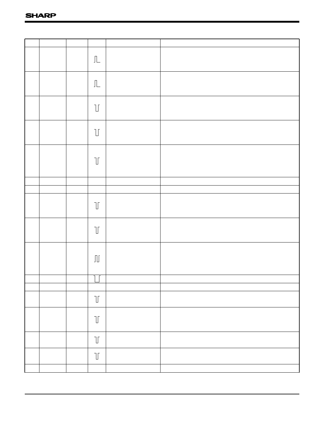
PIN DESCRIPTION
PIN NO. SYMBOL I/O POLARITY
PIN NAME
1 VTAX
O3
Vertical transfer
pulse output 1
2 VTBX
O3
Vertical transfer
pulse output 2
3 VTCX
O3
Vertical transfer
pulse output 3
4 VTDX
O3
Vertical transfer
pulse output 4
5 OFDX
O3
OFD pulse output
6 VDD3
7 GND
8 VHAX
9 VHCX
–
– Power supply
–
– Ground
Readout pulse
O3
output 1
Readout pulse
O3
output 3
10 ID
11 WEN
12 TST1
13 PBLK
14 BCPX
15 BPX
16 CLPX
17 GND
Line index pulse
O3
output
O3
ICD3
O5
O5
Write enable output
– Test pin 1
Pre-blanking pulse
output
Optical black clamp
pulse output
O5
Clamp pulse output
O5
Clamp pulse output
–
– Ground
DESCRIPTION
A vertical transfer pulse for CCD.
Connect to V1AX pin of the vertical driver IC.
For details, see "CONNECTION OF VERTICAL TRANSFER PULSES".
A vertical transfer pulse for CCD.
Connect to V2AX pin of the vertical driver IC.
For details, see "CONNECTION OF VERTICAL TRANSFER PULSES".
A vertical transfer pulse for CCD.
Connect to V3AX pin of the vertical driver IC.
For details, see "CONNECTION OF VERTICAL TRANSFER PULSES".
A vertical transfer pulse for CCD.
Connect to V4AX pin of the vertical driver IC.
For details, see "CONNECTION OF VERTICAL TRANSFER PULSES".
A pulse that sweeps the charge of the photo-diode
for the electronic shutter. Connect to OFD pin of CCD
through the vertical driver IC and DC offset circuit.
Held at H level at normal mode.
Supply of +3 V power.
A grounding pin.
A pulse that transfers the charge of the photo-diode to
the vertical shift register.
For details, see "CONNECTION OF VERTICAL TRANSFER PULSES".
A pulse that transfers the charge of the photo-diode to
the vertical shift register.
For details, see "CONNECTION OF VERTICAL TRANSFER PULSES".
The pulse is used in color separator. The signal
switches H and L at every line.
H : R color line
L : B color line
Write enable output for low-speed shutter pulse.
A test pin. Set open or to L level in the normal mode.
A pulse that corresponds to the cease period of the
horizontal transfer pulse.
A pulse to clamp the optical black signal.
Output stays low during the absence of effective pixels
within the vertical blanking.
A pulse to clamp the signal. The phase is same as BCPX
(pin 14). This pulse is continuous at horizontal cycle.
A pulse to clamp the dummy outputs of CCD. The pulse
stays high during the sweep-out period.
A grounding pin.
3
Share Link: 