LTC1414 データシートの表示(PDF) - Linear Technology
部品番号
コンポーネント説明
メーカー
LTC1414 Datasheet PDF : 20 Pages
| |||
LTC1414
APPLICATIONS INFORMATION
CONVERSION DETAILS
The LTC1414 uses a successive approximation algorithm
and an internal sample-and-hold circuit to convert an
analog signal to a 14-bit parallel output. The ADC is
complete with a precision reference and an internal clock.
The device is easy to interface with microprocessors and
DSPs. (Please refer to the Digital Interface section for the
data format.)
Conversion start is controlled by the CONVST input. At the
start of the conversion the successive approximation
register (SAR) is reset. Once a conversion cycle has begun
it cannot be restarted.
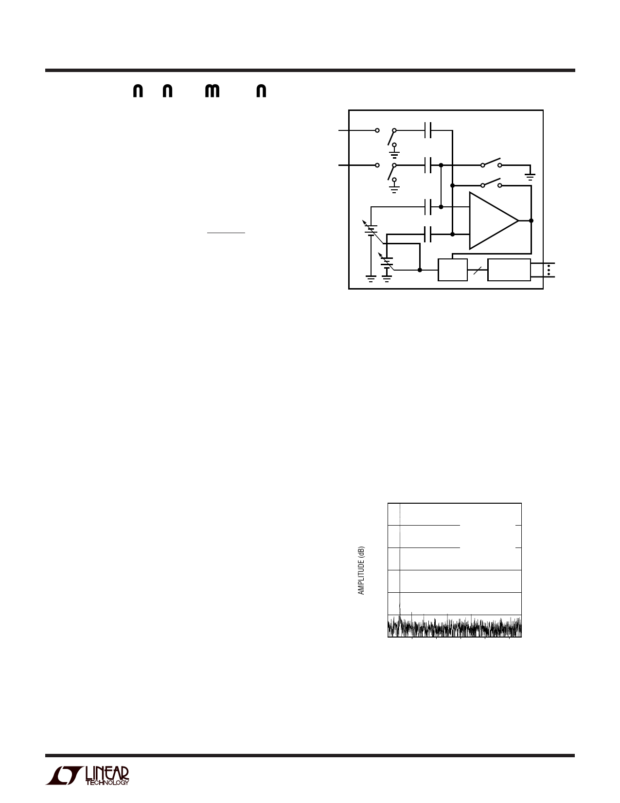
During the conversion, the internal differential 14-bit
capacitive DAC output is sequenced by the SAR from the
most significant bit (MSB) to the least significant bit
(LSB). Referring to Figure 1, the AIN+ and AIN– inputs are
connected to the sample-and-hold capacitors (CSAMPLE)
during the acquire phase, and the comparator offset is
nulled by the zeroing switches. In this acquire phase, a
minimum delay of 70ns will provide enough time for the
sample-and-hold capacitors to acquire the analog signal.
During the convert phase the comparator zeroing switches
open, putting the comparator into compare mode. The
input switches connect the CSAMPLE capacitors to ground,
transferring the differential analog input charge onto the
summing junction. This input charge is successively com-
pared with the binary-weighted charges supplied by the
differential capacitive DAC. Bit decisions are made by the
high speed comparator. At the end of a conversion, the
differential DAC output balances the AIN+ and AIN– input
charges. The SAR contents (a 14-bit data word) which
represents the difference of AIN+ and AIN– are loaded into
the 14-bit output latches.
DYNAMIC PERFORMANCE
The LTC1414 has excellent high speed sampling capabil-
ity. FFT (Fast Four Transform) test techniques are used to
test the ADC’s frequency response, distortion and noise at
the rated throughput. By applying a low distortion sine
wave and analyzing the digital output using an FFT algo-
rithm, the ADC’s spectral content can be examined for
frequencies outside the fundamental. Figure 2 shows a
typical LTC1414 FFT plot.
SAMPLE
AIN+
SAMPLE
AIN–
CSAMPLE+
HOLD
CSAMPLE–
HOLD
CDAC+
VDAC+
CDAC–
ZEROING SWITCHES
HOLD
HOLD
+
COMP
–
VDAC–
SAR
14
OUTPUT
LATCH
Figure 1. Simplified Block Diagram
D13
D0
1414 F01
Signal-to-Noise Ratio
The signal-to-(noise + distortion) ratio [S/(N + D)] is the
ratio between the RMS amplitude of the fundamental input
frequency to the RMS amplitude of all other frequency
components at the A/D output. The output is band limited
to frequencies from above DC and below half the sampling
frequency. Figure 2a shows a typical spectral content with
a 2.2MHz sampling rate and a 100kHz input. The dynamic
performance is excellent for input frequencies up to and
beyond the Nyquist limit of 1.1MHz. (See Figure 2b)
0
SINAD = 80dB
–20
SFDR = 96dB
fSAMPLE = 2.2MHz
–40
fIN = 97.753kHz
–60
–80
–100
–120
0
200 400 600 800 1000
FREQUENCY (kHz)
1414 F02a
Figure 2a. LTC1414 Nonaveraged, 2048 Point FFT,
Input Frequency = 100kHz
7
Share Link: 