PIC16C505T-20/SL データシートの表示(PDF) - Microchip Technology
部品番号
コンポーネント説明
メーカー
PIC16C505T-20/SL Datasheet PDF : 85 Pages
| |||
PIC16C505
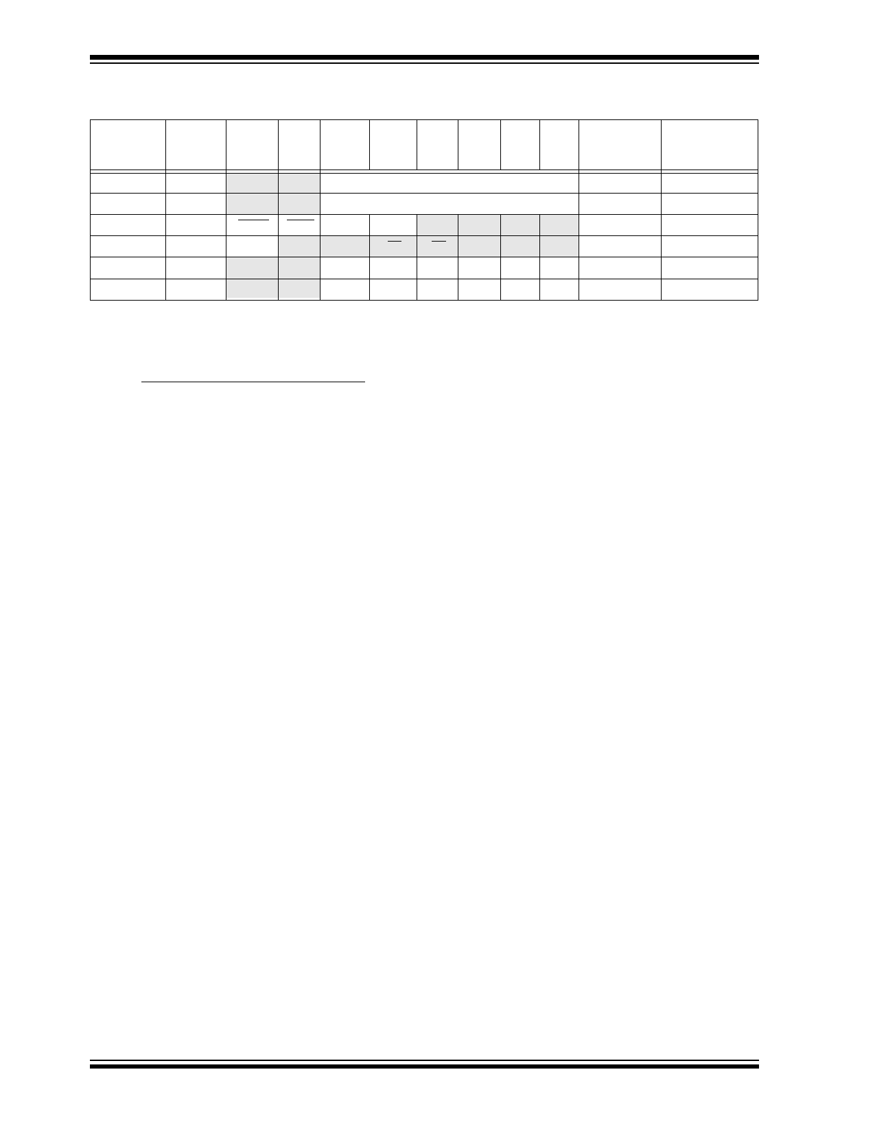
TABLE 5-1: SUMMARY OF PORT REGISTERS
Address
Name
Bit 7
Bit 6 Bit 5
Bit 4 Bit 3 Bit 2 Bit 1 Bit 0
Value on
Power-On
Reset
Value on
All Other Resets
N/A
TRISB
—
— I/O control registers
--11 1111 --11 1111
N/A
TRISC
—
— I/O control registers
--11 1111 --11 1111
N/A
OPTION
RBWU RBPU TOCS TOSE PSA PS2 PS1 PS0 1111 1111
1111 1111
03h
STATUS
RBWUF —
PAO
TO
PD
Z
DC
C
0001 1xxx q00q quuu(1)
06h
PORTB
—
—
RB5
RB4 RB3 RB2 RB1 RB0 --xx xxxx
--uu uuuu
07h
PORTC
—
—
RC5
RC4 RC3 RC2 RC1 RC0 --xx xxxx
--uu uuuu
Legend: Shaded cells not used by Port Registers, read as ‘0’, — = unimplemented, read as ‘0’, x = unknown, u = unchanged,
q = depends on condition.
Note 1: If reset was due to wake-up on pin change, then bit 7 = 1. All other rests will cause bit 7 = 0.
5.5 I/O Programming Considerations
5.5.1 BI-DIRECTIONAL I/O PORTS
Some instructions operate internally as read followed
by write operations. The BCF and BSF instructions, for
example, read the entire port into the CPU, execute
the bit operation and re-write the result. Caution must
be used when these instructions are applied to a port
where one or more pins are used as input/outputs. For
example, a BSF operation on bit5 of PORTB will cause
all eight bits of PORTB to be read into the CPU, bit5 to
be set and the PORTB value to be written to the output
latches. If another bit of PORTB is used as a bi-
directional I/O pin (say bit0) and it is defined as an
input at this time, the input signal present on the pin
itself would be read into the CPU and rewritten to the
data latch of this particular pin, overwriting the
previous content. As long as the pin stays in the input
mode, no problem occurs. However, if bit0 is switched
into output mode later on, the content of the data latch
may now be unknown.
Example 5-1 shows the effect of two sequential read-
modify-write instructions (e.g., BCF, BSF, etc.) on an
I/O port.
A pin actively outputting a high or a low should not be
driven from external devices at the same time in order
to change the level on this pin (“wired-or”, “wired-
and”). The resulting high output currents may damage
the chip.
EXAMPLE 5-1: READ-MODIFY-WRITE
INSTRUCTIONS ON AN
I/O PORT
;Initial PORTB Settings
; PORTB<5:3> Inputs
; PORTB<2:0> Outputs
;
;
PORTB latch PORTB pins
;
---------- ----------
BCF PORTB, 5 ;--01 -ppp --11 pppp
BCF PORTB, 4 ;--10 -ppp --11 pppp
MOVLW 007h
;
TRIS PORTB
;--10 -ppp --11 pppp
;
;Note that the user may have expected the pin
;values to be --00 pppp. The 2nd BCF caused
;RB5 to be latched as the pin value (High).
5.5.2 SUCCESSIVE OPERATIONS ON I/O
PORTS
The actual write to an I/O port happens at the end of
an instruction cycle, whereas for reading, the data
must be valid at the beginning of the instruction cycle
(Figure 5-2). Therefore, care must be exercised if a
write followed by a read operation is carried out on the
same I/O port. The sequence of instructions should
allow the pin voltage to stabilize (load dependent)
before the next instruction causes that file to be read
into the CPU. Otherwise, the previous state of that pin
may be read into the CPU rather than the new state.
When in doubt, it is better to separate these
instructions with a NOP or another instruction not
accessing this I/O port.
DS40192C-page 20
© 1999 Microchip Technology Inc.
Share Link: 