LZ2336 データシートの表示(PDF) - Sharp Electronics
部品番号
コンポーネント説明
メーカー
LZ2336
Sharp Electronics

LZ2336 Datasheet PDF : 8 Pages
| |||
LZ2336
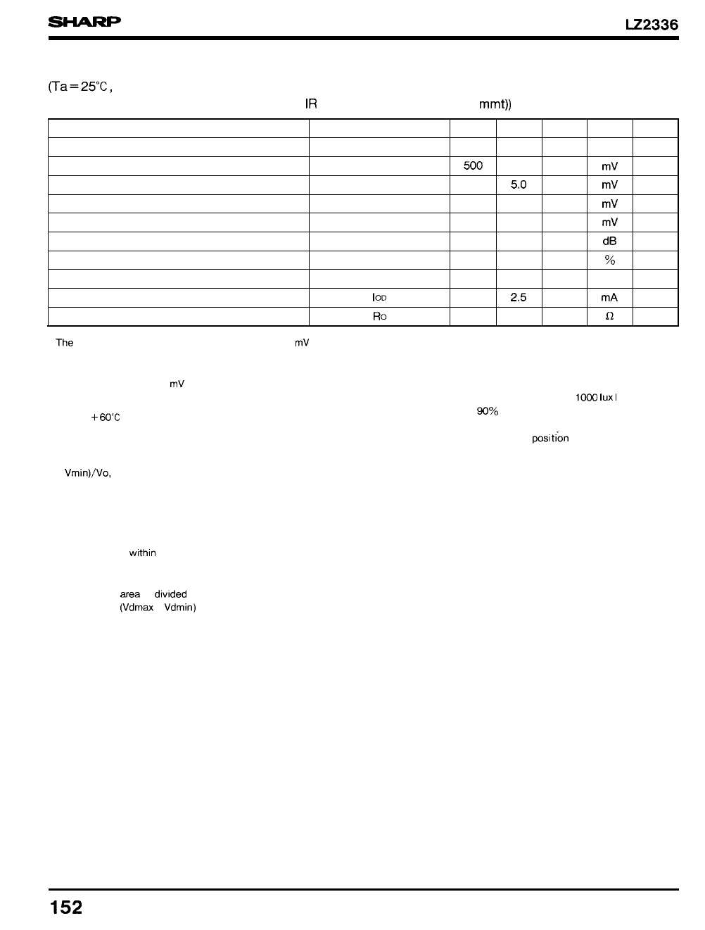
ELECTRICAL CHARACTERISTICS (Drive method : Field Accumulation)
(Ta=25°C, Operating conditions : typical values for the recommended operating conditions, Color
temperature of light source : 3200 K / IR cut-off filter (CM-500, 1 mmt))
PARAMETER
Photo response non-uniformity
Saturation signal
Dark output voltage
Dark signal non-uniformity
Sensitivity
Smear ratio
Image lag
Blooming suppression ratio
Output transistor drain current
Output impedance
SYMBOL
PRNU
Vsat
Vdark
DSNU
R
SMR
Al
ABL
iOD
Ro
MIN.
500
160
1000
TYP.
5.0
1.5
220
– 85
2.5
400
MAX.
15
15.0
5.0
– 76
1.0
5.0
UNIT
‘?/0
mV
mV
mV
mV
dB
0/0
mA
Q
NOTE
2
3
1, 4
1, 5
6
7
8
9
. Tt?e standard output voltage is defined as 150 mV by the
average output voltage under uniform illumination.
q The standard exposure level is defined when the average
output voltage is 150 mV under uniform illumination.
NOTES :
1. Ta : +60CC
2. The image area is divided into 10x 10 segments. The seg-
ment’s voltage is the average output voltage of all the
pixels within the segment. PRNU is defined by (Vmax –
Vmin)/Vo, where Vmax and Vmin are the maximum and
the minimum values of each segment’s voltage respec-
tively, when the average output voltage Vo is 150mV.
3. The image area is divided into 10x 10 segments.
The saturation signal is defined as the minimum of each
segment’s voltage which is the average output voltage of
all the pixels with!n the segment, when the exposure level
is set as 10 times, compared to standard level,
4. The average output voltage under a non-exposure condition.
5. The image ~ea is d!vlded into 10x 10 segments. DSNU is
defined by (Vdmex – Vdmin) under the non-exposure con-
dition where Vdmax and Vdmin are the maximum and the
minimum values of each segment’s voltage, respectively,
that is the average output voltage over all pixels in the
segment.
6 The average output voltage when a 10W Iux I ight source
attached with a 90”A reflector is imaged by a lens of F4,
f50 mm.
7 The sensor is adjusted to poslt(on a V/l O square at the
center of image area where V is the vertical length of the
image area, SMR is defined by the ratio of the output
voltage detected during the vertical blanking period to the
maximum of the pixel voltage in the V/l O square.
8 The sensor is exposed at the exposure level correspond-
ing to the standard condition preceding non-exposure con-
dition. Al is defined by the ratio between the output volt-
age measured at the 1st field during the non-exposure
period and the standard output voltage.
9 The sensor is adjusted to position a V/l O square at the
center of image area. ABL is the ratio between the ex-
posure at the standard condition and the exposure at a
point where a blooming is observed.
152
Share Link: