LT1192CS8 データシートの表示(PDF) - Linear Technology
部品番号
コンポーネント説明
メーカー
LT1192CS8 Datasheet PDF : 12 Pages
| |||
TYPICAL PERFOR A CE CHARACTERISTICS
Slew Rate vs Temperature
600
VS = ±5V
TA = 25°C
RL = 1k
VO = ±2V
–SLEW RATE
500
+SLEW RATE
400
Output Voltage Step
vs Settling Time, AV = – 5
4
VS = ±5V
TA = 25°C
RL = 1k
2
10mV
1mV
0
–2
10mV
1mV
300
–50 –25
0 25 50 75 100 125
TEMPERATURE (°C)
LT1192 • TPC19
Large-Signal Transient Response
–4
20 40
60 80 100 120 140 160
SETTLING TIME (ns)
LT1192 • TPC20
Small-Signal Transient Response
LT1192
Output Voltage Step
vs Settling Time, AV = 5
4
2
10mV
1mV
0
–2
–4
50
10mV
1mV
VS = ±5V
TA = 25°C
RL = 1k
100
150
200
SETTLING TIME (ns)
LT1192 • TPC21
Output Overload
LT1192 • TPC22
AV = 5, CL = 10pF SCOPE PROBE
LT1192 • TPC23
AV = 5, SMALL-SIGNAL RISE TIME,
WITH FET PROBES
AV = 10, VIN = 1.2VP-P
LT1192 • TPC24
APPLICATIO S I FOR ATIO
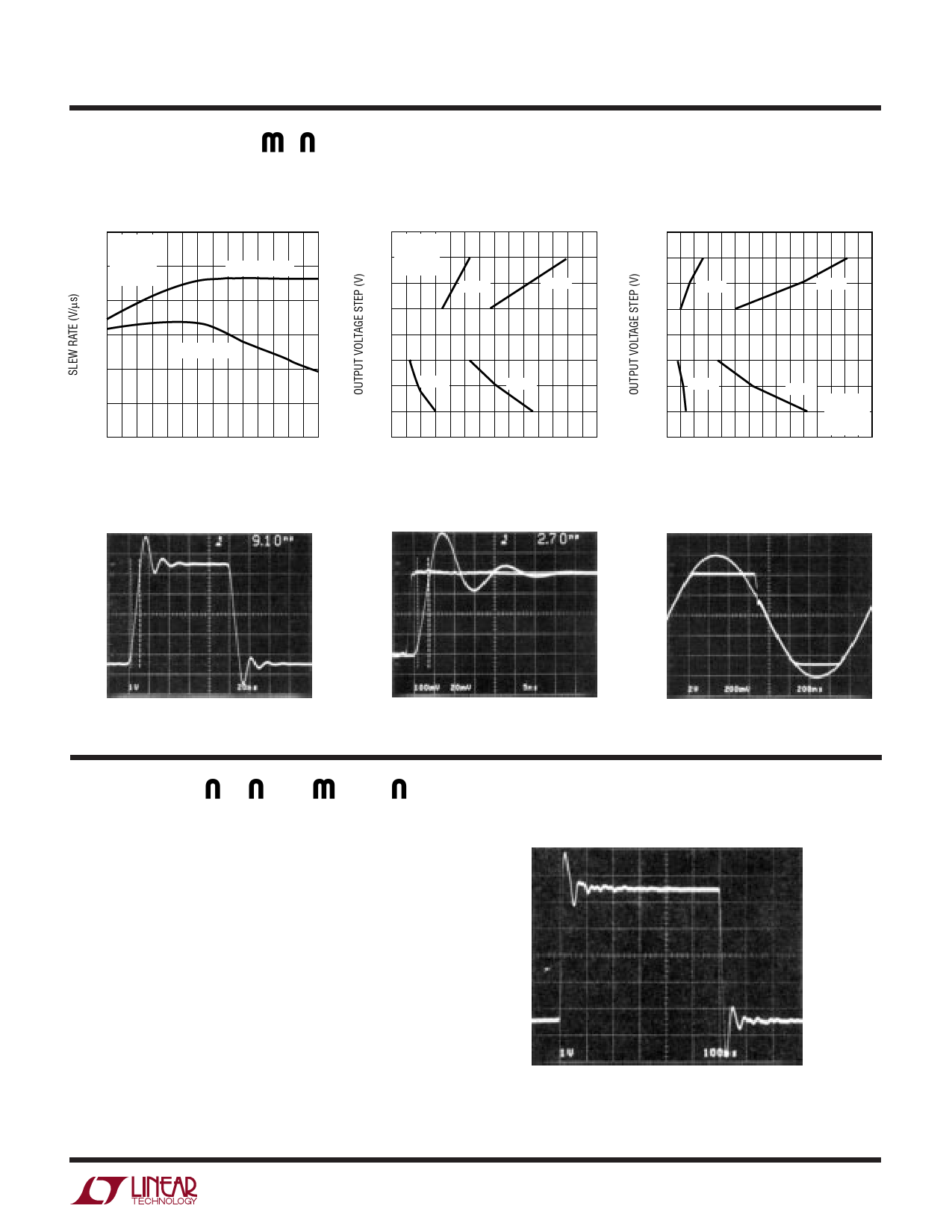
Power Supply Bypassing
The LT1192 is quite tolerant of power supply bypassing.
In some applications a 0.1µF ceramic disc capacitor
placed 1/2 inch from the amplifier is all that is required. A
scope photo of the amplifier output with no supply by-
passing is used to demonstrate this bypassing tolerance,
RL = 1k.
In most applications, and those requiring good settling
time, it is important to use multiple bypass capacitors. A
0.1µF ceramic disc in parallel with a 4.7µF tantalum is
recommended. Two oscilloscope photos with different
bypass conditions are used to illustrate the settling time
characteristics of the amplifier. Note that although the
output waveform looks acceptable at 1V/DIV, when
No Supply Bypass Capacitors
AV = – 5, IN DEMO BOARD, RL = 1k
LT1192 • TA04
7
Share Link: 