SN74LS195AD データシートの表示(PDF) - ON Semiconductor
部品番号
コンポーネント説明
メーカー
SN74LS195AD Datasheet PDF : 8 Pages
| |||
SN74LS195A
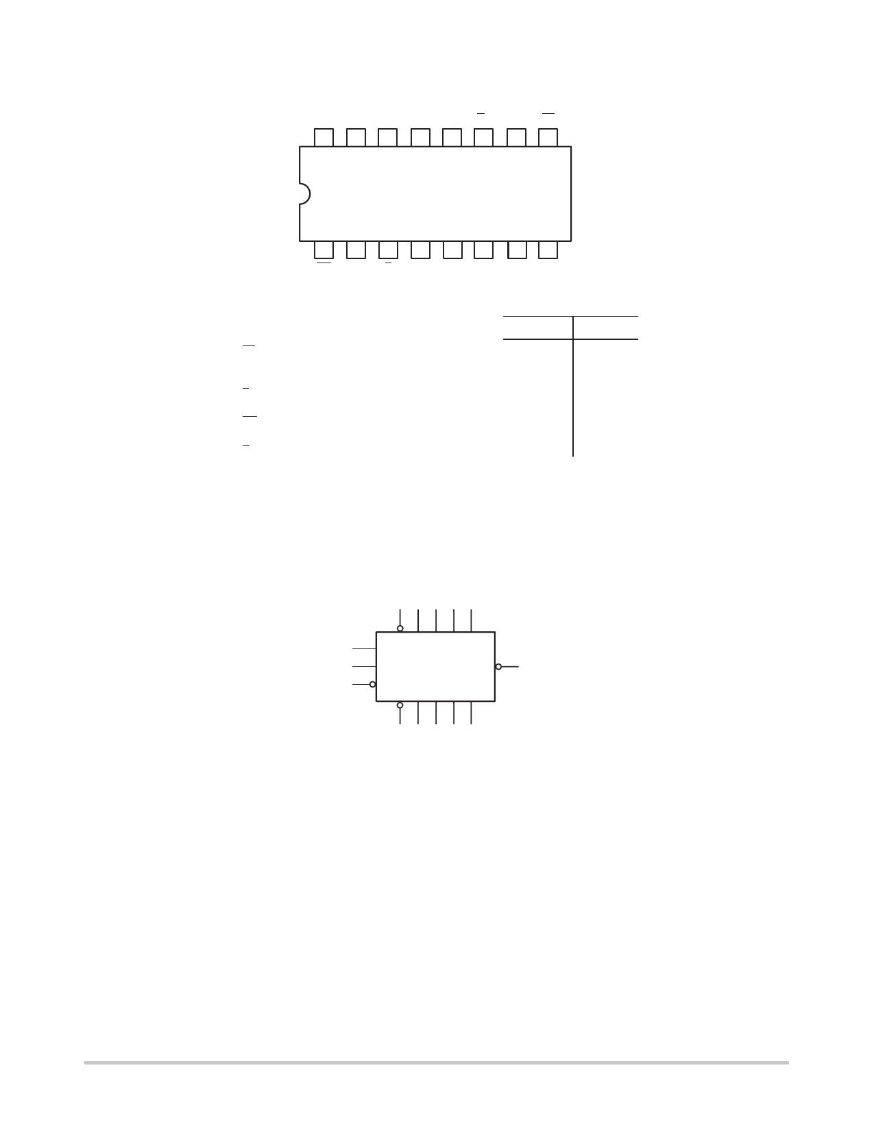
CONNECTION DIAGRAM DIP (TOP VIEW)
VCC Q0 Q1 Q2 Q3 Q3 CP PE
16 15 14 13 12 11 10 9
NOTE:
The Flatpak version has the same
pinouts (Connection Diagram) as
the Dual In-Line Package.
1 2 3 4 56 78
MR J K P0 P1 P2 P3 GND
PIN NAMES
PE
P0 – P3
J
K
CP
MR
Q0 – Q3
Q3
Parallel Enable (Active LOW) Input
Parallel Data Inputs
First Stage J (Active HIGH) Input
First Stage K (Active LOW) Input
Clock (Active HIGH Going Edge) Input
Master Reset (Active LOW) Input
Parallel Outputs
Complementary Last Stage Output
NOTES:
a) 1 TTL Unit Load (U.L.) = 40 mA HIGH/1.6 mA LOW.
LOADING (Note a)
HIGH
LOW
0.5 U.L.
0.5 U.L.
0.5 U.L.
0.5 U.L.
0.5 U.L.
0.5 U.L.
10 U.L.
10 U.L.
0.25 U.L.
0.25 U.L.
0.25 U.L.
0.25 U.L.
0.25 U.L.
0.25 U.L.
5 U.L.
5 U.L.
LOGIC SYMBOL
9456 7
2
J PE P0 P1 P2 P3
10
CP
Q3
11
3
K MR Q0 Q1 Q2 Q3
1 15 14 13 12
VCC = PIN 16
GND = PIN 8
http://onsemi.com
2
Share Link: 