ZXBM2001(2002) データシートの表示(PDF) - Zetex => Diodes
部品番号
コンポーネント説明
メーカー
ZXBM2001 Datasheet PDF : 8 Pages
| |||
ZXBM2001
ZXBM2002 ZXBM2003
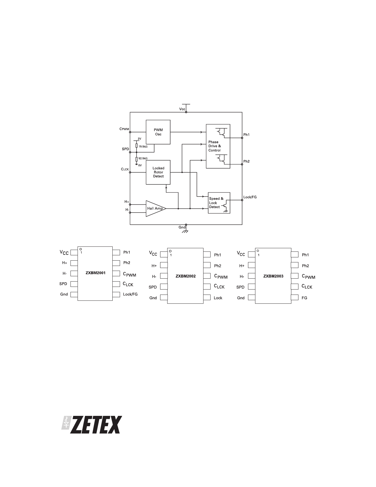
Pin Functional Descriptions
1. VCC - Applied voltage
5. GND - Ground
This is the device supply voltage. For 5V to 12V fans this
can be supplied directly from the Fan Motor supply. For
fans likely to run in excess of the 18V maximum rating
for the device this will be supplied from an external
regulator such as a zener diode.
2. H+
3. H-
- Hall input
- Hall input
The rotor position of the Fan Motor is detected by a Hall
sensor whose output is applied to these pins. This
sensor can be either a 4 pin ‘naked’ Hall device or a 3
pin buffered switching type. For a 4 pin device the
differential Hall output signal is connected to the H+
and H- pins. For a 3 pin buffered Hall sensor the Hall
device output is attached to the H+ pin whilst the H- pin
has an external potential divider attached to hold the
pin at half VCC. When H+ is high in relation to H- Ph2 is
the active drive.
4. SPD - Speed control voltage input
This pin provides control over the Fan Motor speed by
varying the Pulse Width Modulated (PWM) drive ratio
at the Ph1 and Ph2 outputs. This control signal can take
the form of either a voltage input of nominal range 2V
to 1V, representing 0% to 100% drive respectively, or
alternatively a thermistor can be attached to this pin to
control the voltage. The pin has an internal potential
divider between Gnd and an internal 2.0V reference
designed to hold the pin at approximately 1.5V. This
will represent a drive of nominally 50%. The addition of
a 100k NTC thermistor to ground, for example, will
provide a drive nominally 70% at 25°C and 100% at
50°C.
If speed control is not required this pin is can be left
open circuit for 50% drive or tied to ground by a 10k⍀
resistor to provide 100% drive.
If required this pin can also be used as an enable pin.
The application of a voltage of 2.0V to VCC will to force
the PWM drive fully off, in effect disabling the drive.
This is the device supply ground return pin and will
generally be the most negative supply pin to the fan.
6. LOCK/FG - Locked Rotor error output /
Frequency Generator (speed) output
On the ZXBM2001 the Lock/FG pin is designed to be a
dual function pin to provide an indication of the Fans
rotational speed together with an indication of when
the Fan has failed rotating for whatever reason (Rotor
Locked condition). The pin is an open collector drive,
that is there is an active pull down with the high level
being provided by an external pull up resistor. Under
correct operating conditions, and with this external
pull-up in place, this pin will provide an output signal
whose frequency will be twice that of the rotational
frequency of the fan. Should the fan itself stop rotating
for any reason, i.e. an obstruction in the fan blade or a
seized bearing, then the device will enter a Rotor
Locked condition. In this condition the Lock/FG pin will
go high (regardless of the state of the Hall sensor)
when the CLCK pin reaches the VTHH threshold and will
remain high until the fan blades start rotating again.
On the ZXBM2002 variant this pin is Lock. During
normal operation the signal will be low and during a
Locked Rotor condition the pin will go high when the
CLCK pin reaches the VTHH threshold.
For the ZXBM2003 variant this pin is FG. This signal is a
buffered and inverted output of the Hall signal and
therefore provides an output signal whose frequency
will be twice that of the rotational frequency of the fan.
7. CLCK - Locked Rotor timing capacitor
When in a Locked Rotor condition as described above
the Ph1 and Ph2 drive outputs go into a safe drive mode
to protect the external drive devices and the motor
windings. This condition consists of driving the motor
for a short period then waiting for a longer period
before trying again. The frequency at which this takes
place is determined by the size of the capacitor applied
to this CLCK pin. For a 12V supply a value of 1.0uF will
typically provide an ‘On’ (drive) period of 0.33s and an
‘Off’ (wait) period of 4.0s, giving an On:Off ratio of 1:12.
ISSUE 1 - APRIL 2002
4
Share Link: 