CA723 データシートの表示(PDF) - Harris Semiconductor
部品番号
コンポーネント説明
メーカー
CA723 Datasheet PDF : 8 Pages
| |||
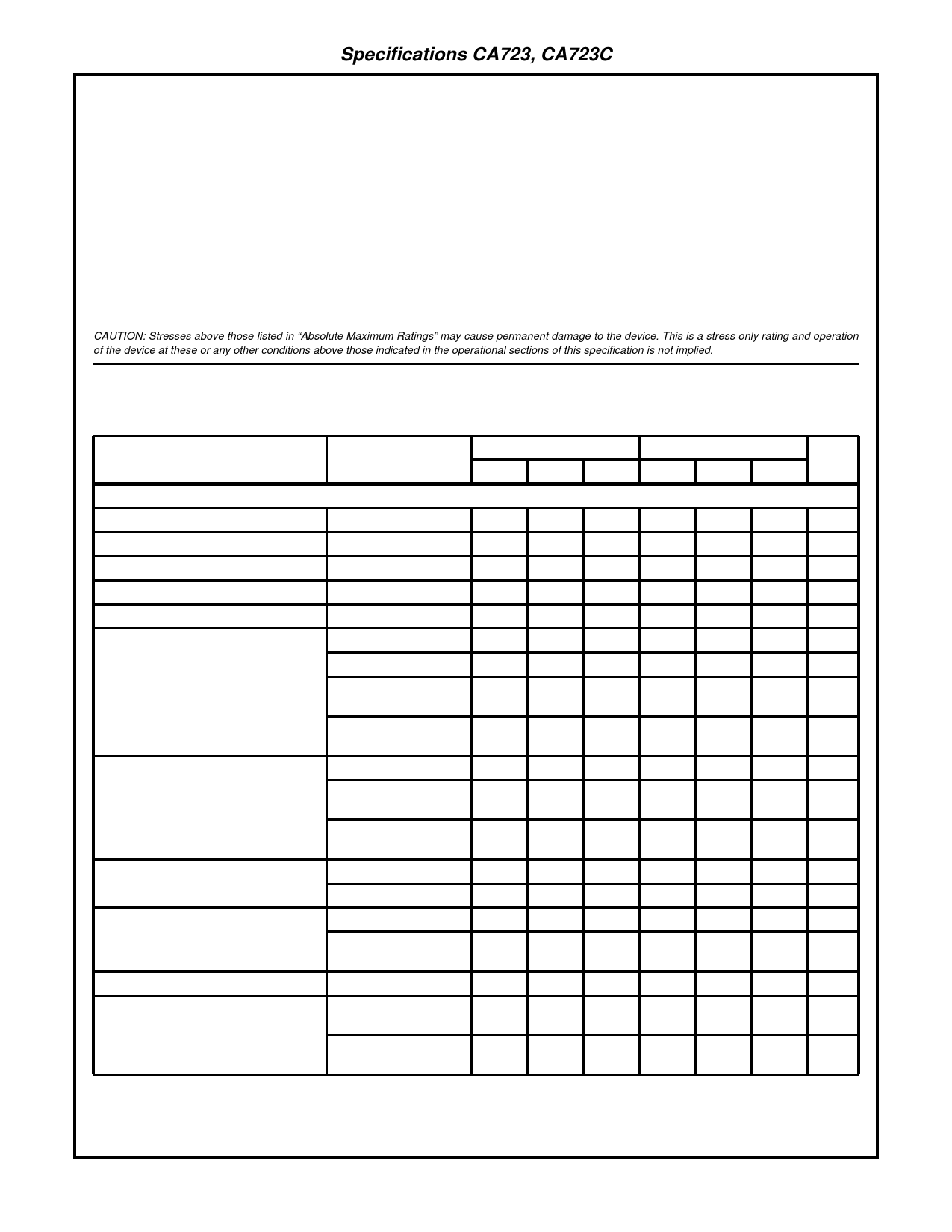
Specifications CA723, CA723C
Absolute Maximum Ratings
Operating Conditions
DC Supply Voltage . . . . . . . . . . . . . . . . . . . . . . . . . . . . . . . . . . . 40V
(Between V+ and V- Terminals)
Pulse Voltage for 50ms
Pulse Width (Between V+ and V- Terminals) . . . . . . . . . . . . . 50V
Differential Input-Output Voltage . . . . . . . . . . . . . . . . . . . . . . . . 40V
Differential Input Voltage
Between Inverting and Noninverting Inputs . . . . . . . . . . . . . . . . ±5V
Between Noninverting Input and V- . . . . . . . . . . . . . . . . . . . . . 8V
Current From Zener Diode Terminal (VZ) . . . . . . . . . . . . . . . . . 25mA
Thermal Resistance
θJA
Plastic DIP Package . . . . . . . . . . . . . . . . 120oC/W
Metal Can . . . . . . . . . . . . . . . . . . . . . . . . 136oC/W
θJC
-
65oC/W
Device Dissipation
CA723T, CA723CT, Up to TA = +25oC. . . . . . . . . . . . . . . . 900mW
CA723E, CA723CE, Up to TA = +25oC . . . . . . . . . . . . . . 1000mW
CA723T, CA723CT, Above TA = +25oC . . . . . . . . . . . . . 7.4mW/oC
CA723E, CA723CE, Above TA = +25oC . . . . . . . . . . . . 8.3mW/oC
Ambient Temperature Range
Operating Temperature Range . . . . . . . . . . . . . . -55oC to +125oC
Storage Temperature Range . . . . . . . . . . . . . . . . -65oC to +150oC
Lead Temperature, During Soldering . . . . . . . . . . . . . . . . . . +265oC
At a distance 1/16” ± 1/32” (1.59mm ± 0.79mm) from case for 10s
max
CAUTION: Stresses above those listed in “Absolute Maximum Ratings” may cause permanent damage to the device. This is a stress only rating and operation
of the device at these or any other conditions above those indicated in the operational sections of this specification is not implied.
DC Electrical Specifications
TA = +25oC, V+ = VC = VI = 12V, V- = 0, VO = 5V, IL = 1mA, C1 = 100pF, CREF = 0, RSCP = 0,
Unless Otherwise Specified. Divider impedance R1 R2 ÷ R1 + R2 at noninverting input, Terminal 5 =
10kΩ. (Figure 20)
CA723
CA723C
PARAMETERS
TEST CONDITION
MIN
TYP
MAX
MIN
TYP
MAX UNITS
DC CHARACTERISTICS
Quiescent Regulator Current, IQ
IL = 0, VI = 30V
Input Voltage Range, VI
Output Voltage Range, VO
Differential Input-Output Voltage, VI - VO
Reference Voltage, VREF
Line Regulation (Note 1)
VI = 12V to 40V
VI = 12V to 15V
VI = 12V to 15V,
TA = -55oC to +125oC
VI = 12V to 15V,
TA = 0oC to +70oC
Load Regulation (Note 1)
IL = 1mA to 50mA
IL = 1mA to 50mA,
TA = -55oC to +125oC
Output-Voltage Temperature Coeffi-
cient, ∆VO
IL = 1mA to 50mA,
TA = 0oC to +70oC
TA = -55oC to +125oC
TA = 0oC to +70oC
Ripple Rejection (Note 2)
f = 50Hz to 10kHz
-
2.3
3.5
-
2.3
4
mA
9.5
-
40
9.5
-
40
V
2
-
37
2
-
37
V
3
-
38
3
-
38
V
6.95
7.15
7.35
6.8
7.15
7.5
V
-
0.02
0.2
-
0.01
0.1
-
-
0.3
-
0.1
0.5 % VO
-
0.01
0.1 % VO
-
-
-
% VO
-
-
-
-
-
0.3
% VO
-
0.03
0.15
-
0.03
0.2 % VO
-
-
0.6
-
-
-
% VO
-
-
-
-
-
0.6
% VO
-
0.002 0.015
-
-
-
%/oC
-
-
-
-
0.003 0.015 %/oC
-
74
-
-
74
-
dB
f = 50Hz to 10kHz,
CREF = 5µF
-
86
-
-
86
-
dB
Short Circuit Limiting Current, ILIM
RSCP = 10Ω, VO = 0
-
65
-
-
65
-
mA
Equivalent Noise RMS Output Voltage, BW = 100Hz to 10kHz,
-
-20
-
VN (Note 2)
CREF = 0
-
20
-
µV
BW = 100Hz to 10kHz,
-
2.5
-
CREF = 5µF
-
2.5
-
µV
NOTES:
1. Line and load regulation specifications are given for condition of a constant chip temperature. For high dissipation condition, temperature
drifts must be separately taken into account.
2. For CREF (See Figure 20)
7-4
Share Link: 