CA723C データシートの表示(PDF) - Intersil
部品番号
コンポーネント説明
メーカー
CA723C Datasheet PDF : 9 Pages
| |||
CA723, CA723C
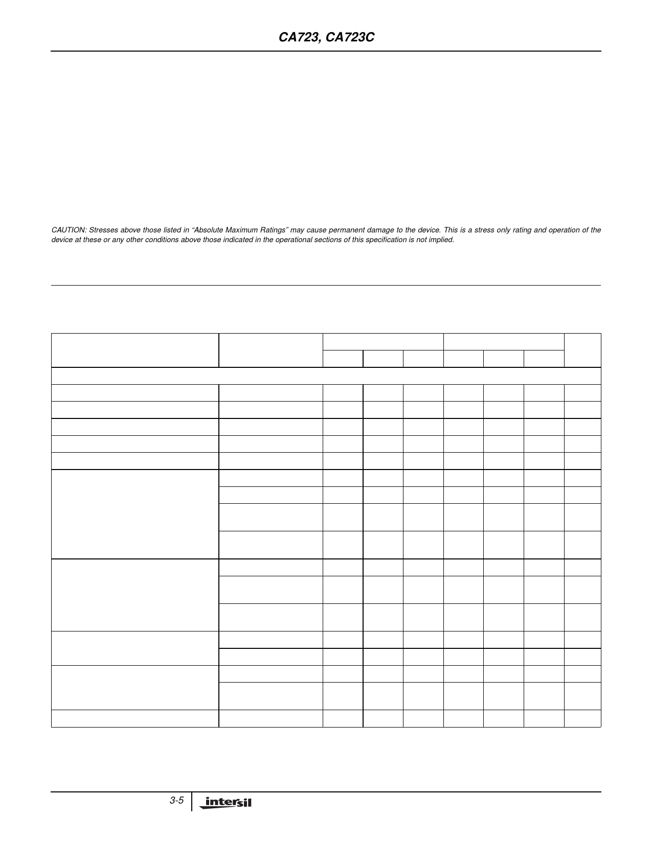
Absolute Maximum Ratings
DC Supply Voltage. . . . . . . . . . . . . . . . . . . . . . . . . . . . . . . . . . . .40V
(Between V+ and V- Terminals)
Pulse Voltage for 50ms
Pulse Width (Between V+ and V- Terminals) . . . . . . . . . . . . . .50V
Differential Input-Output Voltage . . . . . . . . . . . . . . . . . . . . . . . . .40V
Differential Input Voltage
Between Inverting and Noninverting Inputs . . . . . . . . . . . . . . ±5V
Between Noninverting Input and V- . . . . . . . . . . . . . . . . . . . . . .8V
Current From Zener Diode Terminal (VZ) . . . . . . . . . . . . . . . . 25mA
Operating Conditions
Temperature Range . . . . . . . . . . . . . . . . . . . . . . . -55oC to 125oC
Thermal Information
Thermal Resistance (Typical, Note 1)
θJA (oC/W) θJC (oC/W)
PDIP Package . . . . . . . . . . . . . . . . . . . 120
N/A
Metal Can. . . . . . . . . . . . . . . . . . . . . . . 136
65
Device Dissipation
CA723T, Up to TA = 25oC
CA723E, CA723CE, Up to
CA723T, Above TA = 25oC
....
TA =
....
.....
25oC
.....
.
.
.
.
.
.
.
.
.
.
.
.
.
.
.
.
.
.
.
.
.
.
.
.
.
.
.
.
.
.
.
.
.
.
.
.
.
.
.
. . .900mW
. .1000mW
7.4mW/oC
CA723E, CA723CE, Above TA = 25oC . . . . . . . . . . . . 8.3mW/oC
Maximum Storage Temperature Range . . . . . . . . . . -65oC to 150oC
Maximum Lead Temperature, During Soldering . . . . . . . . . . 265oC
At a distance 1/16” ± 1/32” (1.59mm ± 0.79mm) from case
for 10s Max
CAUTION: Stresses above those listed in “Absolute Maximum Ratings” may cause permanent damage to the device. This is a stress only rating and operation of the
device at these or any other conditions above those indicated in the operational sections of this specification is not implied.
NOTE:
1. θJA is measured with the component mounted on an evaluation PC board in free air.
DC Electrical Specifications
TA = 25oC, V+ = VC = VI = 12V, V- = 0, VO = 5V, IL = 1mA, C1 = 100pF, CREF = 0, RSCP = 0,
Unless Otherwise Specified. Divider impedance R1 R2 ÷ R1 + R2 at noninverting input,
Terminal 5 = 10kΩ. (Figure 20)
CA723
CA723C
PARAMETER
TEST CONDITION
MIN
TYP
MAX
MIN
TYP
MAX
DC CHARACTERISTICS
Quiescent Regulator Current, IQ
Input Voltage Range, VI
Output Voltage Range, VO
Differential Input-Output Voltage, VI - VO
Reference Voltage, VREF
Line Regulation (Note 2)
Load Regulation (Note 2)
Output-Voltage Temperature Coefficient,
∆VO
Ripple Rejection (Note 3)
IL = 0, VI = 30V
VI = 12V to 40V
VI = 12V to 15V
VI = 12V to 15V,
TA = -55oC to 125oC
VI
TA
=
=
12V
0oC
to
to
15V,
70oC
IL = 1mA to 50mA
IL = 1mA to 50mA,
TA = -55oC to 125oC
IL = 1mA to 50mA,
TA = 0oC to 70oC
TA = -55oC to 125oC
TA = 0oC to 70oC
f = 50Hz to 10kHz
-
2.3
3.5
-
2.3
4
9.5
-
40
9.5
-
40
2
-
37
2
-
37
3
-
38
3
-
38
6.95
7.15
7.35
6.8
7.15
7.5
-
0.02
0.2
-
0.1
0.5
-
0.01
0.1
-
0.01
0.1
-
-
0.3
-
-
-
-
-
-
-
-
0.3
-
0.03
0.15
-
0.03
0.2
-
-
0.6
-
-
-
-
-
-
-
-
0.6
-
0.002 0.015
-
-
-
-
-
-
-
0.003 0.015
-
74
-
-
74
-
Short Circuit Limiting Current, ILIM
f = 50Hz to 10kHz,
CREF = 5µF
RSCP = 10Ω, VO = 0
-
86
-
-
65
-
-
86
-
-
65
-
UNITS
mA
V
V
V
V
% VO
% VO
% VO
% VO
% VO
% VO
% VO
%/oC
%/oC
dB
dB
mA
3-5
Share Link: 