LC74793 データシートの表示(PDF) - SANYO -> Panasonic
部品番号
コンポーネント説明
メーカー
LC74793 Datasheet PDF : 24 Pages
| |||
LC74793, 74793JM
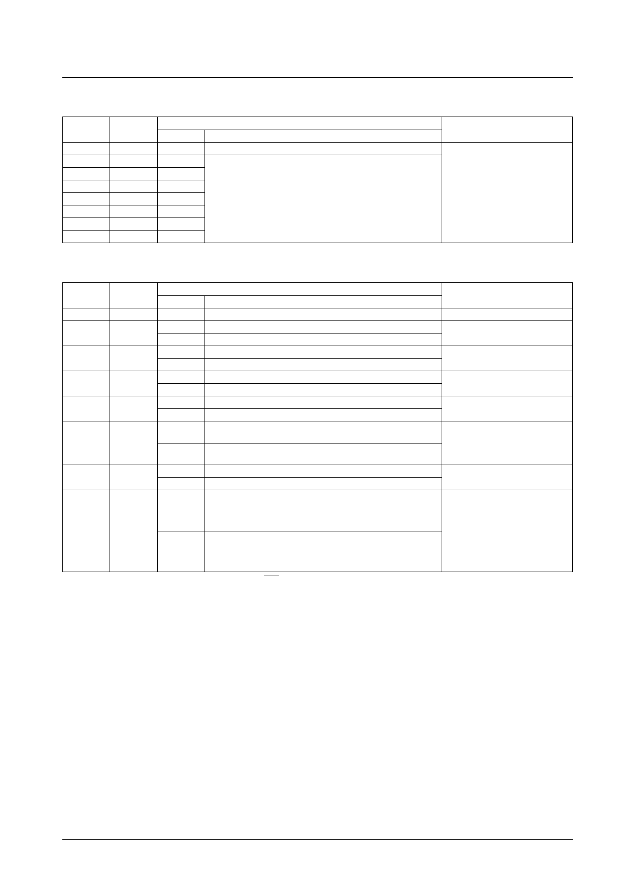
Command 2 (VPS/PDC control command 2)
• First byte
DA 0 to 7
7
6
5
4
3
2
1
0
Register
—
—
—
—
—
—
—
—
Status
1
1
1
1
0
0
1
0
Contents
Function
First byte identification bit
Command 2 identification code.
VPS/PDC control settings 2.
Notes
• Second byte
DA 0 to 7
7
6
Register
—
VMWSE2
5
VMWSEL
4
HBS2
3
HBS1
2
BMS
1
EMS
0
DCE
Status
0
0
1
0
1
0
1
0
1
0
1
0
1
0
1
Contents
Function
Second byte identification bit
From the vertical mask period start return period
From 10H before the vertical mask period start return period
The vertical mask period is the return period
The vertical mask period is 9H
Clock run discrimination 1 (2 times)
Clock run discrimination 2 (4 times)
Framing code discrimination 1
Framing code discrimination 2 (A single bad bit is ignored)
Error check enabled (The error check can be turned on or off on
per-byte basis.)
Error check disabled (Applications can select whether data with errors
is held or written for each byte.)
Data hold
Data write (Error bits are set to 0 in VPS mode)
Error check turned on for unused bytes
VPS: bytes 3, 4, and 6 to 10, PDC: bytes 7 to 12
Header 1: bytes 14 to 37, 2: 14 to 29, 3 14 to 21.
Status 1 (3): bytes 7 to 25, status 2 (4) bytes 7 to 35.
Error check turned off for unused bytes
VPS: bytes 3, 4, and 6 to 10, PDC: bytes 7 to 12
Header 1: bytes 14 to 37, 2: 14 to 29, 3 14 to 21.
Status 1 (3): bytes 7 to 25, status 2 (4) bytes 7 to 35.
Notes
CPOUT pin vertical mask period
switching 2
CPOUT pin vertical mask period
switching
Clock run discrimination circuit setting
Framing code discrimination selection
When set to 0: If there are no errors in bytes
for which the error check is turned on, those
bytes will be written to P-S (COM7-9).
When set to 1: Data is written to P-S
regardless of whether or not errors occurred.
When error checking is enabled, specifies the
processing when an error occurs in a byte for
which error checking was turned off
Error check setting for unused data
bytes
Biphase (VPS),
Hamming (PDC),
Odd parity (header)
Note: All registers are cleared to 0 when the IC is reset by the RST pin.
No. 5966-10/24
Share Link: 