LTC1042M データシートの表示(PDF) - Linear Technology
部品番号
コンポーネント説明
メーカー
LTC1042M Datasheet PDF : 8 Pages
| |||
LTC1042
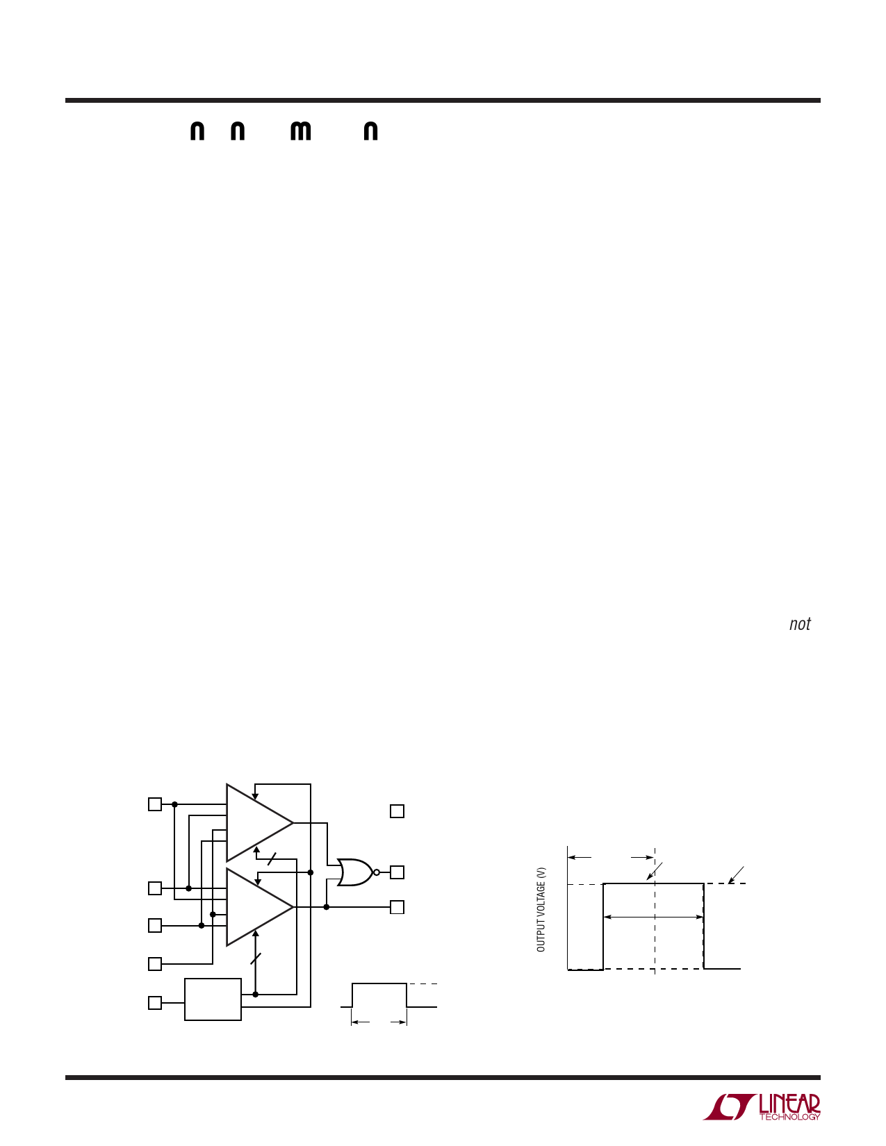
APPLICATIO S I FOR ATIO
The LTC1042 uses sampled data techniques to achieve its
unique characteristics. It consists of two comparators,
each of which has two differential inputs (Figure 1). When
the sum of the voltages on a comparator’s inputs is
positive, the output is high; when the sum is negative, the
output is low. The inputs are interconnected such that
when (CENTER – WIDTH/2) ≤ VIN ≤ (CENTER + WIDTH/2)
both comparator outputs are low. In this condition VIN is
within the window and the WITHIN WINDOW output is
high. When VIN > CENTER + WIDTH/2, VIN is above the
window and the ABOVE WINDOW output is high.
An important feature of the LTC1042 is the non-interaction
of the inputs. This means the center and width of the
window can be changed without one affecting the other.
Also note that the width of the window is set by a ground
referred signal WlDTH/2).
Strobing
An internal oscillator allows the LTC1042 to strobe itself.
The frequency of oscillation sets the sampling rate and is
set with an external RC network (see typical curve, OSC
frequency vs REXT, CEXT). To assure oscillation, under all
conditions, REXT must be between 100kΩ and 10MΩ.
There is no limit to the size of CEXT.
A sampling cycle is initiated on the positive going transi-
tion of the voltage on the OSC pin. When this voltage is
near the positive supply, a Schmitt trigger trips and
initiates the sampling cycle. A sampling cycle consists of
applying power to both comparators, sampling the inputs,
storing the results in CMOS output latches and turning the
power off. This whole process takes approximately 80µs.
During the 80µs “active” time, the LTC1042 draws
typically 1.2mA (lS(ON)) at V+ = 5V. Because power is
consumed only during the “active” time, extremely low
average power consumption can be achieved at low sample
rates. For example, at a sample rate of 1 sample/second
the average power consumption is:
Power = (V+) (IS(AVG)) = 5V • 1.2mA • 80µs/1sec
= 0.48µW
At low sampling rates, REXT dominates the power con-
sumption. REXT consumes power continuously. The aver-
age voltage at the OSC pin is approximately V+/2. The
power consumed by REXT is:
P(REXT) = (V+/2)2REXT
Example: Assume REXT = 1MΩ and V+ = 5V. Then:
P(REXT) = (2.5)2/1MΩ = 6.25µW
This is more than ten times the typical power consumed by
the LTC1042 at V+ = 5V and 1 sample/second. Where
power is a premium, REXT should be made as large as
possible. Note that the power dissipated by REXT is not a
function of the sampling frequency or CEXT.
If high sampling rates are needed and power consumption
is of secondary importance, a convenient way to get the
maximum possible sampling rate is to make REXT = 100kΩ
and CEXT = 0. The sampling rate, set by the LTC1042’s
active time, will nominally be ≈ 10kHz.
WINDOW
CENTER
2
(VIN)
VIN
(WINDOW 3
CENTER)
WIDTH/2 5
GND 4
OSC 7
+
–
+ COMP A
–
4
+
–
+ COMP B
–
4
TIMING
GENERATOR
(A)
4
8 V+
1 WITHIN WINDOW
6
ABOVE WINDOW
(BELOW WINDOW)
WINDOW
CENTER
V+
WITHIN
WINDOW
–WIDTH/2 WIDTH/2
ABOVE
WINDOW
0V
POWER ON
80µs
POWER OFF
Figure 1. LTC1042 Block Diagram
VL
VU
INPUT VOLTAGE, VIN
(B)
LTC1042 • AI01
1042fa
Share Link: 