MC14049BF データシートの表示(PDF) - ON Semiconductor
部品番号
コンポーネント説明
メーカー
MC14049BF Datasheet PDF : 8 Pages
| |||
MC14049B, MC14050B
Hex Buffer
The MC14049B Hex Inverter/Buffer and MC14050B Noninverting
Hex Buffer are constructed with MOS P–Channel and N–Channel
enhancement mode devices in a single monolithic structure. These
complementary MOS devices find primary use where low power
dissipation and/or high noise immunity is desired. These devices
provide logic level conversion using only one supply voltage, VDD.
The input–signal high level (VIH) can exceed the VDD supply
voltage for logic level conversions. Two TTL/DTL loads can be driven
v when the devices are used as a CMOS–to–TTL/DTL converter (VDD
= 5.0 V, VOL 0.4 V, IOL ≥ 3.2 mA).
Note that pins 13 and 16 are not connected internally on these
devices; consequently connections to these terminals will not affect
circuit operation.
• High Source and Sink Currents
• High–to–Low Level Converter
• Supply Voltage Range = 3.0 V to 18 V
• VIN can exceed VDD
• Meets JEDEC B Specifications
• Improved ESD Protection On All Inputs
MAXIMUM RATINGS (Voltages Referenced to VSS) (Note 2.)
Symbol
Parameter
Value
Unit
VDD
DC Supply Voltage Range
Vin
Input Voltage Range
(DC or Transient)
– 0.5 to +18.0
V
– 0.5 to +18.0
V
Vout
Output Voltage Range
(DC or Transient)
– 0.5 to VDD + 0.5
V
Iin
Input Current
(DC or Transient) per Pin
± 10
mA
Iout
Output Current
(DC or Transient) per Pin
± 45
mA
PD
Power Dissipation,
per Package (Note 3.)
(Plastic)
(SOIC)
mW
825
740
TA
Ambient Temperature Range
Tstg
Storage Temperature Range
TL
Lead Temperature
(8–Second Soldering)
– 55 to +125
°C
– 65 to +150
°C
260
°C
2. Maximum Ratings are those values beyond which damage to the device
may occur.
3. Temperature Derating: See Figure 3.
This device contains protection circuitry to protect the inputs against damage
due to high static voltages or electric fields referenced to the VSS pin only. Extra
precautions must be taken to avoid applications of any voltage higher than the
maximum rated voltages to this high–impedance circuit. For proper operation, the
ranges VSS ≤ Vin ≤ 18 V and VSS ≤ Vout ≤ VDD are recommended.
Unused inputs must always be tied to an appropriate logic voltage level (e.g.,
either VSS or VDD). Unused outputs must be left open.
© Semiconductor Components Industries, LLC, 2000
1
March, 2000 – Rev. 3
http://onsemi.com
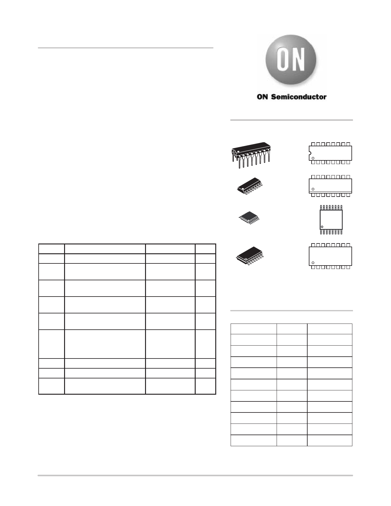
PDIP–16
P SUFFIX
CASE 648
SOIC–16
D SUFFIX
CASE 751B
MARKING
DIAGRAMS
16
MC140XXBCP
AWLYYWW
1
16
140XXB
AWLYWW
1 16
TSSOP–16
DT SUFFIX
CASE 948F
14
0XXB
ALYW
SOEIAJ–16
F SUFFIX
CASE 966
16 1
MC140XXB
AWLYWW
1
XX
= Specific Device Code
A
= Assembly Location
WL or L = Wafer Lot
YY or Y = Year
WW or W = Work Week
ORDERING INFORMATION
Device
Package
Shipping
MC14049BCP
PDIP–16
2000/Box
MC14049BD
SOIC–16
2400/Box
MC14049BDR2 SOIC–16 2500/Tape & Reel
MC14049BF
SOEIAJ–16 See Note 1.
MC14050BCP
PDIP–16
2000/Box
MC14050BD
SOIC–16
2400/Box
MC14050BDR2 SOIC–16 2500/Tape & Reel
MC14050BDTEL TSSOP–16 2000/Tape & Reel
MC14050BF
SOEIAJ–16 See Note 1.
MC14050BFEL SOEIAJ–16 See Note 1.
1. For ordering information on the EIAJ version of
the SOIC packages, please contact your local
ON Semiconductor representative.
Publication Order Number:
MC14049B/D
Share Link: 