CC1020-1070DK-433 データシートの表示(PDF) - Unspecified
部品番号
コンポーネント説明
メーカー
CC1020-1070DK-433 Datasheet PDF : 92 Pages
| |||
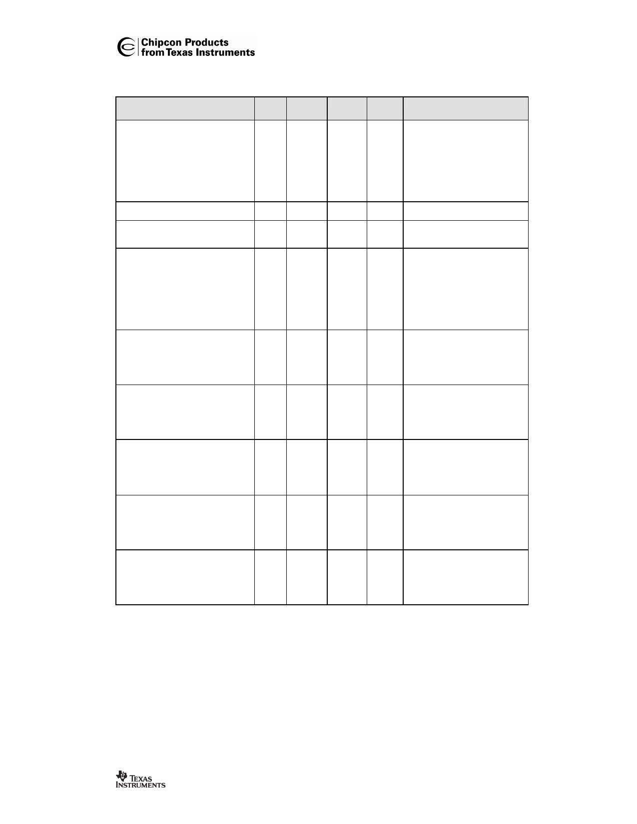
CC1021
Parameter
Spurious reception
LO leakage, 433/868 MHz
VCO leakage
Spurious emission, radiated CW
9 kHz ñ 1 GHz
1 ñ 4 GHz
Input impedance
433 MHz
868 MHz
Matched input impedance, S11
433 MHz
868 MHz
Matched input impedance
433 MHz
868 MHz
Bit synchronization offset
Data latency
NRZ mode
Manchester mode
Min Typ
Max
37
<-80/-66
-64
Unit
Condition / Note
dB
dBm
dBm
Ratio between sensitivity for an
unwanted frequency to the
sensitivity in the wanted channel.
The signal source is swept over
all frequencies 100 MHz ñ 2 GHz.
Signal level for BER = 10 3.
102.4 kHz channel filter
bandwidth.
VCO frequency resides between
1608 ñ 1880 MHz
<-60
<-60
dBm
dBm
Complying with EN 300 220,
FCC CFR47 part 15 and ARIB
STD T-67.
Spurious emissions can be
measured as EIRP values
according to EN 300 220.
58 - j10
54 - j22
Receive mode. See section 14 on
Ω page 46 for details.
Ω
Using application circuit matching
-14
dB network. See section 14 on page
46 for details.
-12
dB
39 - j14
32 - j10
8000
Using application circuit matching
Ω network. See section 14 on page
46 for details.
Ω
ppm The maximum bit rate offset
tolerated by the bit
synchronization circuit for 6 dB
degradation (synchronous modes
only)
Time from clocking the data on
4
Baud the transmitter DIO pin until data
is available on receiver DIO pin
8
Baud
Table 4. RF receive parameters
SWRS045
Page 10 of 91
Share Link: 