33289 データシートの表示(PDF) - Motorola => Freescale
部品番号
コンポーネント説明
メーカー
33289 Datasheet PDF : 10 Pages
| |||
Freescale Semiconductor, Inc.
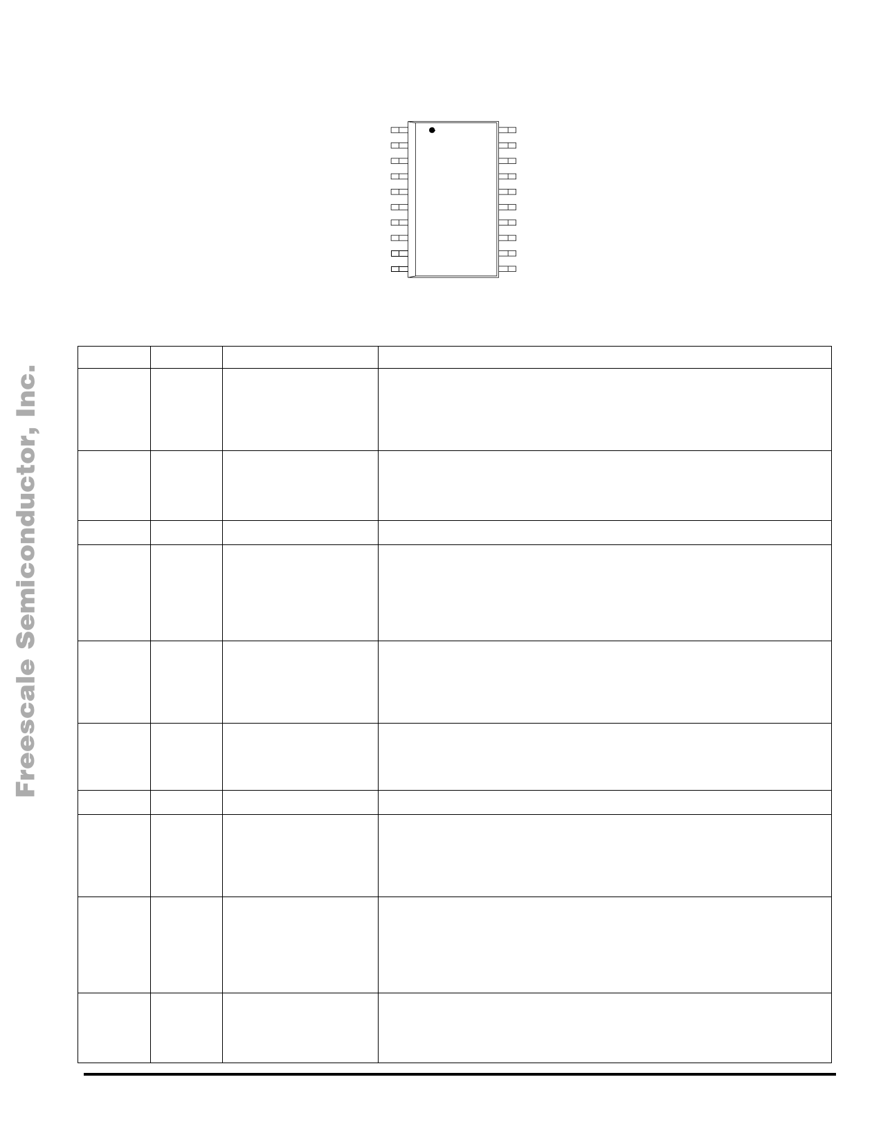
VBAT
1
VBAT
2
OUT1
3
OUT1
4
VBAT
5
VBAT
6
NC
7
IN1
8
ST1
9
OLDE
10
20
VBAT
19
VBAT
18 OUT2
17
OUT2
16
VBAT
15
VBAT
14
NC
13
IN2
12
ST2
11
GND
PIN FUNCTION DESCRIPTION
Pin
Pin Name
Formal Name
1, 2
5, 6
15, 16
19, 20
VBAT
Voltage Supply (Battery)
3, 4
OUT1
Output Channel 1
7, 14
NC
8
IN1
No Connect
Input Channel 1
9
ST1
Status Channel 1
10
OLDE
Open Load Detection
Enable
11
GND
12
ST2
Ground
Status Channel 2
13
IN2
Input Channel 2
17, 18
OUT2
Output Channel 2
Definition
These are the power supply pins of the device. These pins are directly connected with
the lead frame of the package and are tied to the drain of the switching MOSFET. These
pins can be directly connected to the battery voltage. In addition to their supply function,
these pins participate to the thermal behavior of the device in conducting the heat from
the switching MOSFET to the printed circuit board.
These pins are the output one terminals. They connect directly to the source of the
power MOSFET. These pins are used by the control circuitry to sense the device output
voltage. The RDS(ON) is 40 mΩ maximum per output at 25°C and will increase to a
maximum of 75 mΩ at 150°C junction temperature.
These pins do not connect.
These are the device input pins. They control their associated outputs. The levels are
CMOS compatible. When the input is a logic low, the associated output MOSFET is in
the OFF state. When input is high, the MOSFET is turned ON and the load is activated.
When both inputs are low, the device is in Standby mode and its supply current is
reduced. Each input pin has an internal active pull-down, so it will not float if
disconnected.
These pins are the channel one fault detection flags. Their internal structure is an open
drain architecture with an internal clamp at 6.0 V. An external pull-up resistor connected
to VDD (5.0 V) is required. This is an active low output. If the device is in its normal
condition the status lines will be high. If open load or other fault occurs, the associated
channel status flag will be pulled low. Please see Functional Truth Table.
This pin is a digital input, enabling the open load current diagnostic circuitry. When
OLDE is a logic low, the open load circuitry is not powered and the bias current draw of
the device is at a minimum. If OLDE is a logic high, the open load circuitry is functional
at the price of a higher bias current draw. OLDE pin has a pull down resistor.
Ground of the integrated circuit.
These pins are the channel two fault detection flags. Their internal structure is an open
drain architecture with an internal clamp at 6V. An external pull up resistor connected to
Vdd (5.0 V) is needed. This is an active low output. If the device is in its normal condition
the status lines will be high. If open load or other fault occurs, the associated channel
status flag will be pulled low. Please, see Functional Truth Table, Table 1.
These are the device input pins. They control their associated outputs. The levels are
CMOS compatible. When the input is a logic low, the associated output MOSFET is in
the OFF state. When input is high, the MOSFET is turned ON and the load is activated.
When both inputs are low, the device is in Standby mode and its supply current is
reduced. Each input pin has an internal active pull down, so it will not float if
disconnected.
These pins are the output two terminals. They are connected to the source of the power
MOSFET. These pins are used by the control circuitry to sense the device output
voltage. The RDS(ON) is 40 mΩ maximum per output at 25°C and will increase to a
maximum of 75 mΩ at 150°C junction temperature.
MOTOROLA ANALOG INTEGRATED CIFRCoUrITMDoErVeICEInDfAoTrAmation On This Product,
Go to: www.freescale.com
33289
3
Share Link: 