K9LBG08U0D-P データシートの表示(PDF) - Samsung
部品番号
コンポーネント説明
メーカー
K9LBG08U0D-P Datasheet PDF : 74 Pages
| |||
K9HCG08U1D K9PDG08U5D
K9LBG08U0D K9MDG08U5D
Preliminary
FLASH MEMORY
Product Introduction
NAND Flash Memory has addresses multiplexed into 8 I/Os. This scheme dramatically reduces pin counts and allows system
upgrades to future densities by maintaining consistency in system board design. Command, address and data are all written through
I/O's by bringing WE to low while CE is low. Those are latched on the rising edge of WE. Command Latch Enable(CLE) and Address
Latch Enable(ALE) are used to multiplex command and address respectively, via the I/O pins. Some commands require one bus
cycle. For example, Reset Command, Status Read Command, etc. require just one cycle bus. Some other commands, like page read
and block erase and page program, require two cycles: one cycle for setup and the other cycle for execution.. Page Read and Page
Program need the same five address cycles following the required command input. In Block Erase operation, however, only the three
row address cycles are used. Device operations are selected by writing specific commands into the command register. Table 1
defines the specific commands of the K9LBG08U0D.
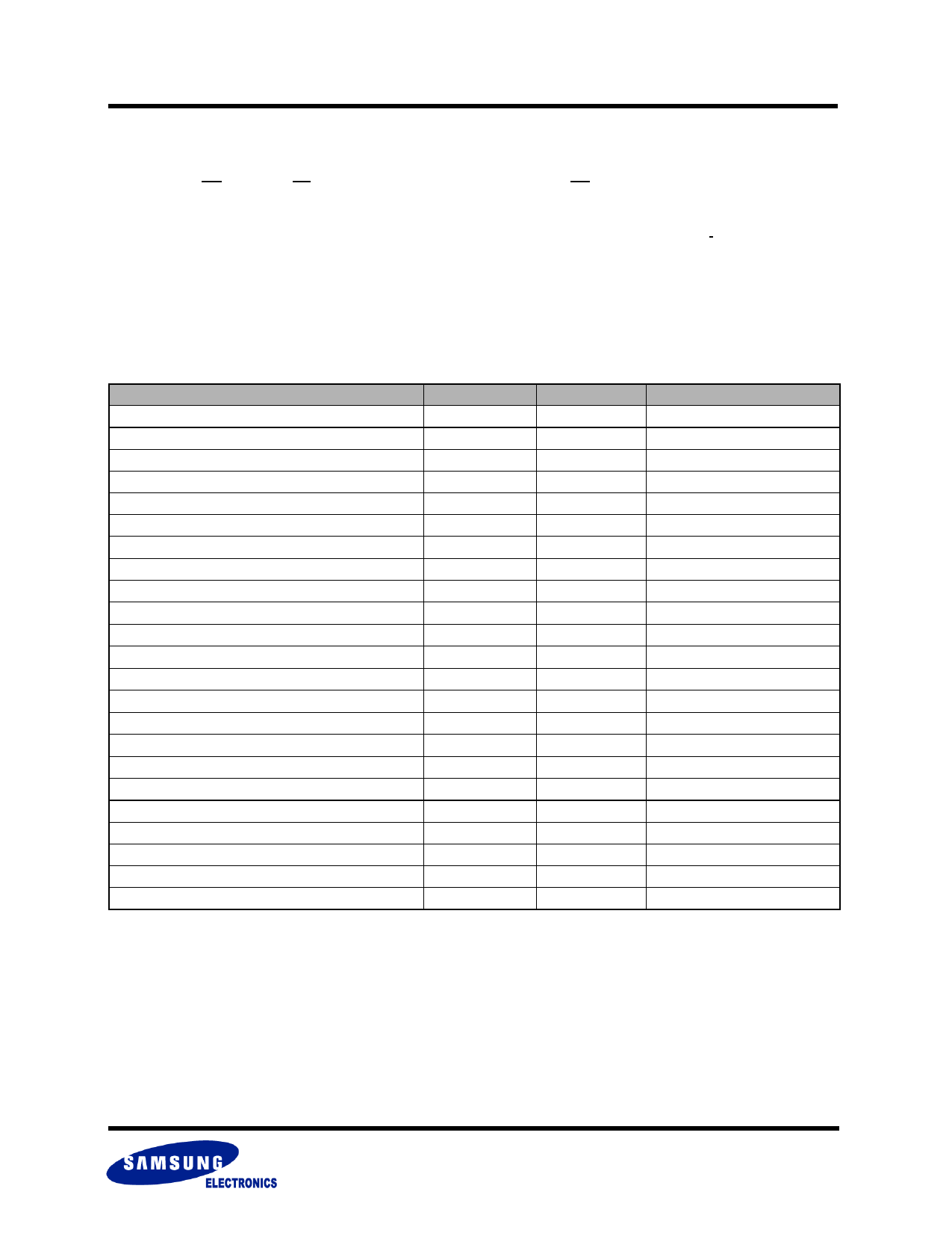
Table 1. Command Sets
Function
Read
Read for Copy Back
Cache Read
Read Start for Last Page Cache Read
Page Program
Cache Program
Copy-Back Program
Block Erase
Random Data Input(1)
Random Data Output(1)
Two-Plane Read (3)
Two-Plane Read for Copy-Back(3)
Two-Plane Random Data Output (1) (3)
Two-Plane Cache Read(3)
Two-Plane Page Program(2)
Two-Plane Copy-Back Program(2)
Two-Plane Cache Program(2)
Two-Plane Block Erase
Read ID
Read Status
Chip1 Status
Chip2 Status
Reset
1st Set
2nd Set
00h
30h
00h
35h
31h
-
3Fh
-
80h
10h
80h
15h
85h
10h
60h
D0h
85h
-
05h
E0h
60h----60h
30h
60h----60h
35h
00h----05h
E0h
60h----60h
33h
80h----11h
81h----10h
85h----11h
81h----10h
80h----11h
81h----15h
60h----60h
D0h
90h
-
70h
-
O
F1h
O
F2h
O
FFh
-
O
NOTE : 1. Random Data Input/Output can be executed in a page.
2. Any command between 11h and 80h/81h/85h is prohibited except 70h/F1h/F2h and FFh.
3. Two-Plane Random Data out must be used after Two-Plane Read or Two-Plane Cache Read operation
4. Interleave-operation between two chips is allowed.
Caution : Any undefined command inputs are prohibited except for above command set of Table 1.
Samsung Confidential
11
Share Link: 