AWT6107 データシートの表示(PDF) - ANADIGICS
部品番号
コンポーネント説明
メーカー
AWT6107 Datasheet PDF : 8 Pages
| |||
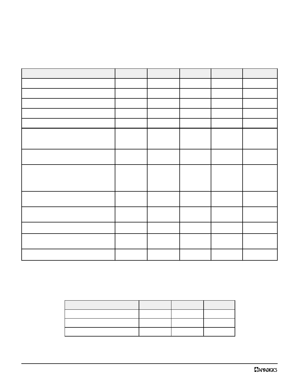
Electrical Specification
DCS:
Test Conditions: VCC = 3.5V, ZIN = ZOUT = 50W, TC = 25°C ± 3, PIN = 8dBm, PWIDTH = 1154ms, Duty Cycle = 25%,
VBAND = HIGH
PARAMETER
Frequency
Control Voltage
Input Power
Output Power DCS (PIN = 8dBm)
Power Added Efficiency
Degraded Output Power
VCC = 3.0V, VAPC = 2.2V,
PIN = 6dBm, TC = 75 °C
Isolation
VAPC = 0.2V, PIN = 8dBm
Harmonics
2nd
3rd
4fo to 12.75GHz
Stability: Load 5:1 VSWR
All phase angles
Ruggedness: PIN = 10 dBm,
VCC = 4.5V, VAPC = 0.2 - 3.0V
Noise Power fo + 20MHz
Switching Time
VAPC on to 90% detected POUT
Input VSWR
SYMBOL
fo
POUT
PIN
POUT
PAE
MIN
1710
6
31.5
29.5
TYP
-
1.6
8
50
-85
Table 6: DCS Electrical Specification
MAX
1785
2.2
10
UNITS
MHz
V
dBm
dBm
%
dBm
-30
dBm
-4
-7
-7
-70 or
-36
8:1 VSWR
All Phases
dBm
dBm
dBm
dBc
dBm
dBm/100 kHz
2
ms
2:1
Logic Level Definitions:
The band select pin (VBAND) is used to select which amplifier will enabled by the voltage applied to the VAPC input.
SIGNAL
MIN
MAX
UNITS
Logic High
2
3
V
Logic Low
0
0.5
V
Input bias current
10
mA
Table 7: Logic Level Definitions
Revison 1, January 2001
4
Share Link: 