ATA01501S2C データシートの表示(PDF) - ANADIGICS
部品番号
コンポーネント説明
メーカー
ATA01501S2C Datasheet PDF : 12 Pages
| |||
PIN
VDD
56pF
GND
56pF
VDD
VDD2
GND
19 I
IIN
GND
GND
1992
VOUT
GND GND GND CBY CBY GND CAGC GND
56pF
56pF
OUT
Figure 4: ATA01501D1C Die Typical Bonding
ATA01501
VDD
NC
12 11 10
0.1µF
NC
1
2
IIN
3
9
NC
8
0.1µF
7
Vout
GND
or
Neg.Supply
4 56
56 pF
56 pF
Figure 5: ATA01501DS2C Typical SQFP
Connection Package
Power Supplies and General Layout
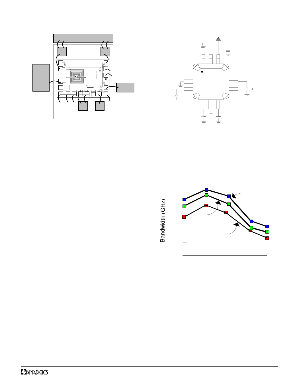
The ATA00501D1C may be operated from a positive
supply as low as +4.5 V and as high as +6.0 V. Below
+4.5 V, bandwidth, overload and sensitivity will
degrade, while at +6.0 V, bandwidth, overload and
sensitivity improve (see Bandwidth vs. Temperature
curves). Use of surface mount (preferably MIM type
capacitors), low inductance power supply bypass
capacitors (>=56pF) are essential for good high
frequency and low noise performance. The power
supply bypass capacitors should be mounted on or
connected to a good low inductance ground plane.
General Layout Considerations
Since the gain stages of the transimpedance
amplifier have an open loop bandwidth in excess
of 1.0 GHz, it is essential to maintain good high
frequency layout practices. To prevent oscillations,
a low inductance RF ground plane should be made
available for power supply bypassing. Traces that
can be made short should be made short, and
the utmost care should be taken to maintain very
low capacitance at the photodiode-TIA interface
(IIN), as excess capacitance at this node will
cause a degradation in bandwidth and sensitivity
(see Bandwidth vs. CT curves).
0.17
0.15
CT = 0.5 pF
VDD = 5.5 V
0.13
0.11
0.90
VDD = 5.0 V
VDD = 4.5 V
-40
10
60 85
Temperature (O C)
Figure 6: Bandwidth vs. Temperature
PRELIMINARY DATA SHEET - Rev 1.6
5
08/2001
Share Link: 