ATA00501 データシートの表示(PDF) - ANADIGICS
部品番号
コンポーネント説明
メーカー
ATA00501 Datasheet PDF : 8 Pages
| |||
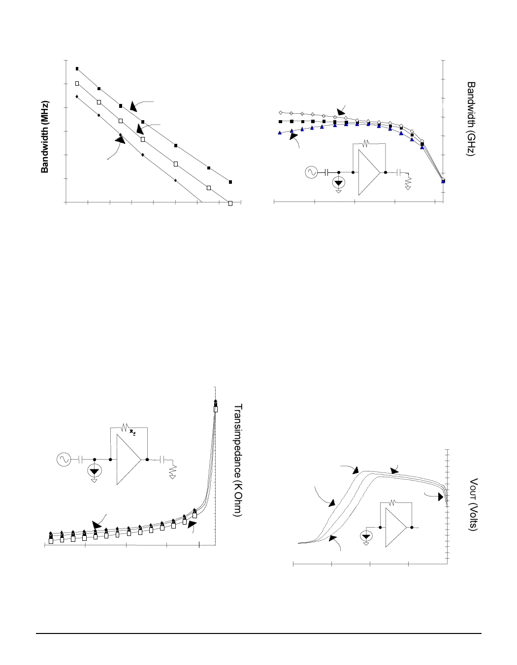
Figure 7: Bandwidth vs. CT
90
B(3dB)≈ A/ 2π Rf (Cin +Ct)
80
70
VDD = 5.5 V
60
VDD= 5.0 V
50
VDD= 4.5 V
40
30
0 0.2 0.4 0.6 0.8 1 1.2
CT(pF)
Note: All performance curves are typical @ TA =25 oC
unless otherwise noted.
IIN Connection
(Refer to the equivalent circuit diagram.) Bonding
the detector cathode to IIN (and thus drawing current
from the ATA00501) improves the dynamic range.
Although the detector may be used in the reverse
direction for input currents not exceeding 25mA, the
specifications for optical overload will not be met.
Figure 8: Transimpedance vs. IIN
25
22
19
16
IIN
50
13
10
VDD = 5.5 V
7
4
VDD = 4.5 V 1
-2.1 -1.6 -1.1 -0.6 -0.1
IIN (mA DC)
ATA00501
Figure 9: Bandwidth vs. IIN
1.44
1.24
VDD = 5.5 V
1.04
.84
VDD = 4.5 V
Rf
IIN
.64
.44
.24
50
.04
- 2.1
- 1.6 - 1.1 - 0.6 - 0.1
IIN (mA DC)
VOUT Connection
The output pad should be connected via a coupling
capacitor to the next stage of the receiver channel
(filter or decision circuits), as the output buffers are
not designed to drive a DC coupled 50 ohm load
(this would require an output bias current of
approximately 36 mA to maintain a quiescent 1.8
Volts across the output load). If VOUT is connected
to a high input impedance decision circuit (>500
ohms), then a coupling capacitor may not be
required, although caution should be exercised
since DC offsets of the photo detector/TIA
combination may cause clipping of subsequent gain
or decision circuits.
Figure 10: VOUT vs. IIN
Output Collapse
Heavy AGC
VDD = 5.5 V
Linear Region
Rf
IIN
VDD = 4.5 V
vOUT
-4
-3
-2
-1
IIN (mA DC)
3.4
3.2
3.0
2.9
2.7
2.5
2.4
(
2.2
2.0
o
1.9
1.7
1.5
1.4
1.2
1.0
0.8
0.7
0.5
0.3
0.2
0.0
PRELIMINARY DATA SHEET - Rev 1.5
5
08/2001
Share Link: 