1032E1111 データシートの表示(PDF) - Lattice Semiconductor
部品番号
コンポーネント説明
メーカー
1032E1111 Datasheet PDF : 16 Pages
| |||
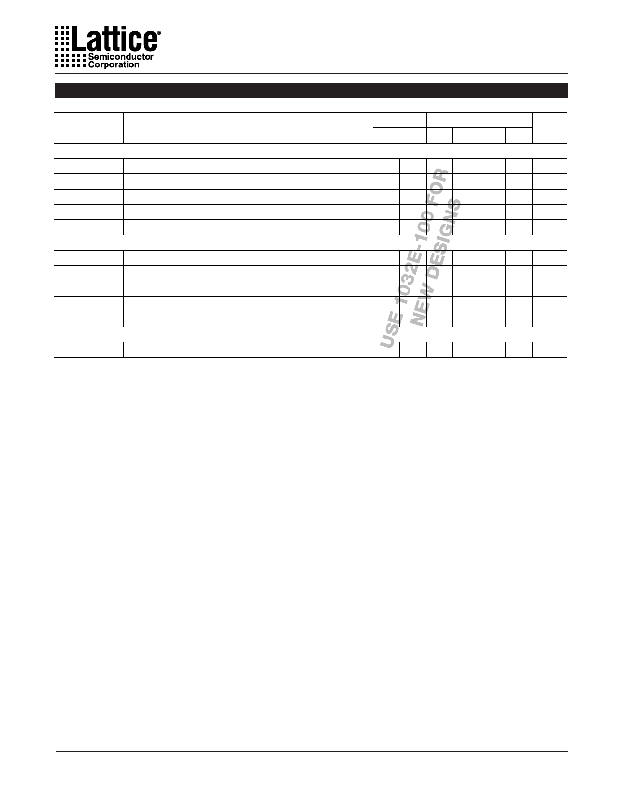
Specifications ispLSI and pLSI 1032E
Internal Timing Parameters1
PARAM. #
DESCRIPTION
Outputs
tob
49 Output Buffer Delay
tsl
50 Output Buffer Delay, Slew Limited Adder
toen
todis
tgoe
51 I/O Cell OE to Output Enabled
52 I/O Cell OE to Output Disabled
53 Global OE
Clocks
tgy0
54 Clock Delay, Y0 to Global GLB Clock Line (Ref. clock)
tgy1/2
tgcp
tioy2/3
55 Clock Delay, Y1 or Y2 to Global GLB Clock Line
56 Clock Delay, Clock GLB to Global GLB Clock Line
57 Clock Delay, Y2 or Y3 to I/O Cell Global Clock Line
tiocp
58 Clock Delay, Clock GLB to I/O Cell Global Clock Line
Global Reset
tgr
59 Global Reset to GLB and I/O Registers
1. Internal Timing Parameters are not tested and are for reference only.
-90
-80
-70
UNITS
MIN. MAX. MIN. MAX. MIN. MAX.
– 1.7 – 2.1 – 2.6 ns
– 10.0 – 10.0 – 10.0 ns
– 5.3 – 5.7 – 6.2 ns
– 5.3 – 5.7 – 6.2 ns
– 3.7 – 4.3 – 5.8 ns
1.4 1.4 1.5 1.5 1.5 1.5 ns
2.4 2.9 2.6 3.1 1.5 1.5 ns
0.8 1.8 0.8 1.8 0.8 1.8 ns
0.0 0.0 0.0 0.0 0.0 0.0 ns
0.8 1.8 0.8 1.8 0.8 1.8 ns
– 4.5
– 4.5 – 4.6 ns
Table 2-0037B/1032E
10
Share Link: 