24C32 データシートの表示(PDF) - Unspecified
部品番号
コンポーネント説明
メーカー
24C32 Datasheet PDF : 10 Pages
| |||
24C32
24C64
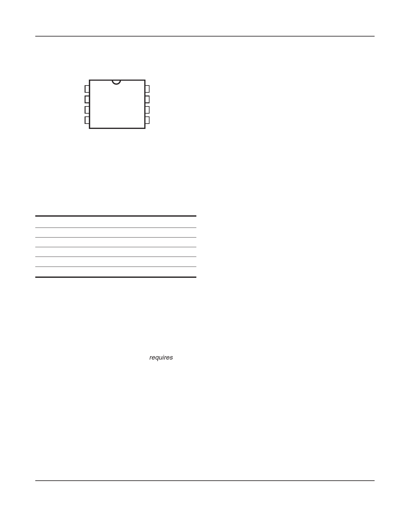
PIN CONFIGURATION
8-Pin DIP, SOIC, TSSOP, and MSOP
A0 1
A1 2
A2 3
GND 4
8 VCC
7 WP
6 SCL
5 SDA
Bookly Micro
PIN DESCRIPTIONS
A0-A2
SDA
SCL
WP
Vcc
GND
Address Inputs
Serial Address/Data I/O
Serial Clock Input
Write Protect Input
Power Supply
Ground
SCL
This input clock pin is used to synchronize the data
transfer to and from the device.
SDA
The SDA is a Bi-directional pin used to transfer addresses
and data into and out of the device. The SDA pin is an open
drain output and can be wire-Ored with other open drain
or open collector outputs. The SDA bus requires a pullup
resistor to Vcc.
A0, A1, A2
The A0, A1 and A2 are the device address inputs that are
hardwired or left not connected for hardware compatibility
with the 24C16. When pins are hardwired, as many as eight
32K/64K devices may be addressed on a single bus
system. When the pins are not hardwired, the default values
of A0, A1, and A2 are zero.
WP
WP is the Write Protect pin. The input level determines if all,
partial, or none of the array is protected from modifications.
www.bookly.com
3
Rev. B
01/09/07
Share Link: 