28C04A データシートの表示(PDF) - Microchip Technology
部品番号
コンポーネント説明
メーカー
28C04A Datasheet PDF : 10 Pages
| |||
28C04A
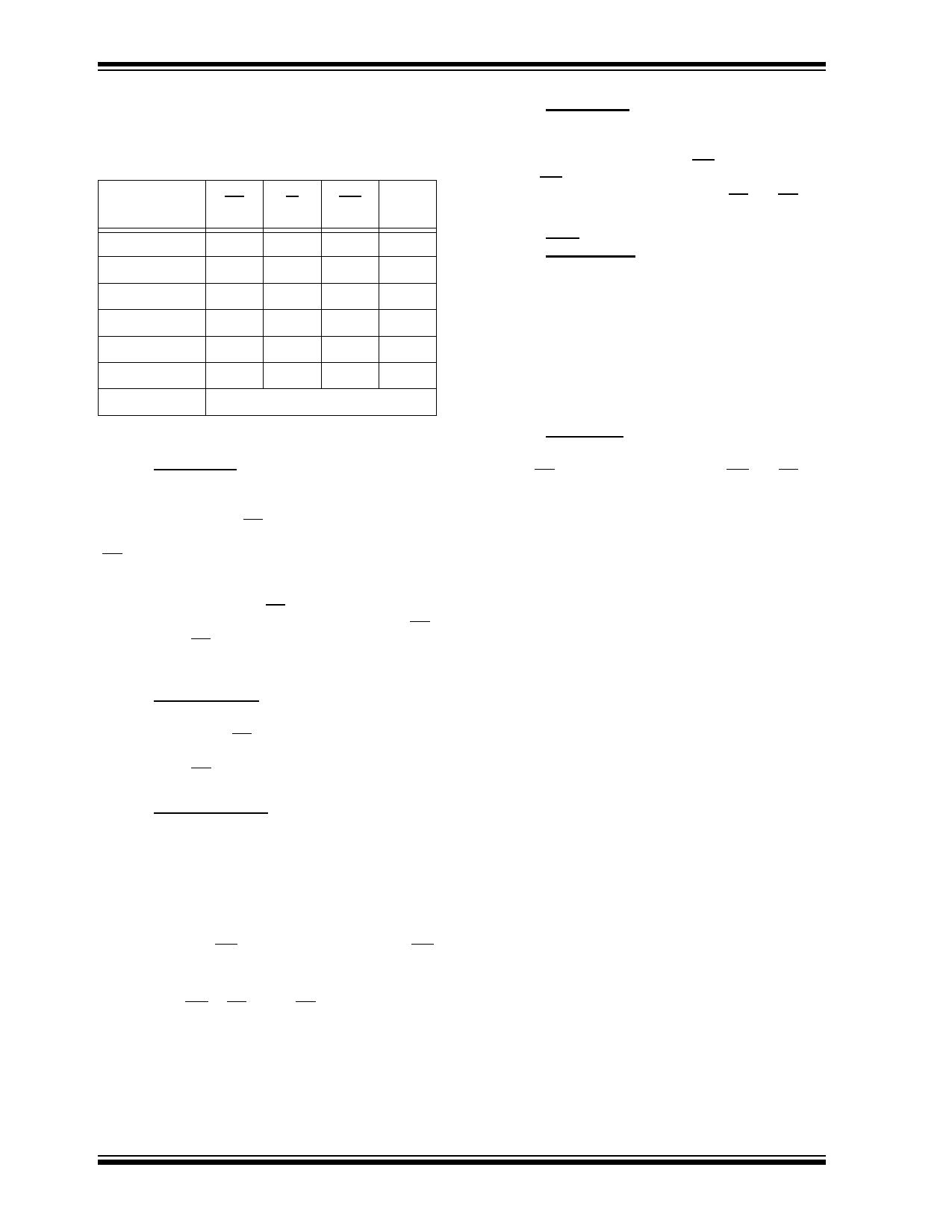
2.0 DEVICE OPERATION
The Microchip Technology Inc. 28C04A has four basic
modes of operation—read, standby, write inhibit, and
byte write—as outlined in the following table.
Operation
Mode
CE
IE
WE
I/O
Read
L
L
H
DOUT
Standby
H
X
X High Z
Write Inhibit
H
X
X High Z
Write Inhibit
X
L
X High Z
Write Inhibit
X
X
H High Z
Byte Write
L
H
L
DIN
Byte Clear
Automatic Before Each “Write”
X = Any TTL level.
2.1 Read Mode
The 28C04A has two control functions, both of which
must be logically satisfied in order to obtain data at the
outputs. Chip enable (CE) is the power control and
should be used for device selection. Output Enable
(OE) is the output control and is used to gate data to the
output pins independent of device selection. Assuming
that addresses are stable, address access time (tACC)
is equal to the delay from CE to output (tCE). Data is
available at the output tOE after the falling edge of OE,
assuming that CE has been low and addresses have
been stable for at least tACC-tOE.
2.2 Standby Mode
The 28C04A is placed in the standby mode by applying
a high signal to the CE input. When in the standby
mode, the outputs are in a high impedance state, inde-
pendent of the OE input.
2.3 Data Protection
In order to ensure data integrity, especially during criti-
cal power-up and power-down transitions, the following
enhanced data protection circuits are incorporated:
First, an internal VCC detect (3.3 volts typical) will inhibit
the initiation of non-volatile programming operation
when VCC is less than the VCC detect circuit trip.
Second, there is a WE filtering circuit that prevents WE
pulses of less than 10 ns duration from initiating a write
cycle.
Third, holding WE or CE high or OE low, inhibits a write
cycle during power-on and power-off (VCC).
2.4 Write Mode
The 28C04A has a write cycle similar to that of a Static
RAM. The write cycle is completely self-timed and initi-
ated by a low going pulse on the WE pin. On the falling
edge of WE, the address information is latched. On ris-
ing edge, the data and the control pins (CE and OE) are
latched.
2.5 Data Polling
The 28C04A features Data polling to signal the comple-
tion of a byte write cycle. During a write cycle, an
attempted read of the last byte written results in the
data complement of I/O7 (I/O0 to I/O6 are indetermin-
able). After completion of the write cycle, true data is
available. Data polling allows a simple read/compare
operation to determine the status of the chip eliminating
the need for external hardware.
2.6 Chip Clear
All data may be cleared to 1's in a chip clear cycle by
raising OE to 12 volts and bringing the WE and CE low.
This procedure clears all data.
DS11126H-page 6
2004 Microchip Technology Inc.
Share Link: 