74LCX374 データシートの表示(PDF) - ON Semiconductor
部品番号
コンポーネント説明
メーカー
74LCX374 Datasheet PDF : 8 Pages
| |||
MC74LCX374
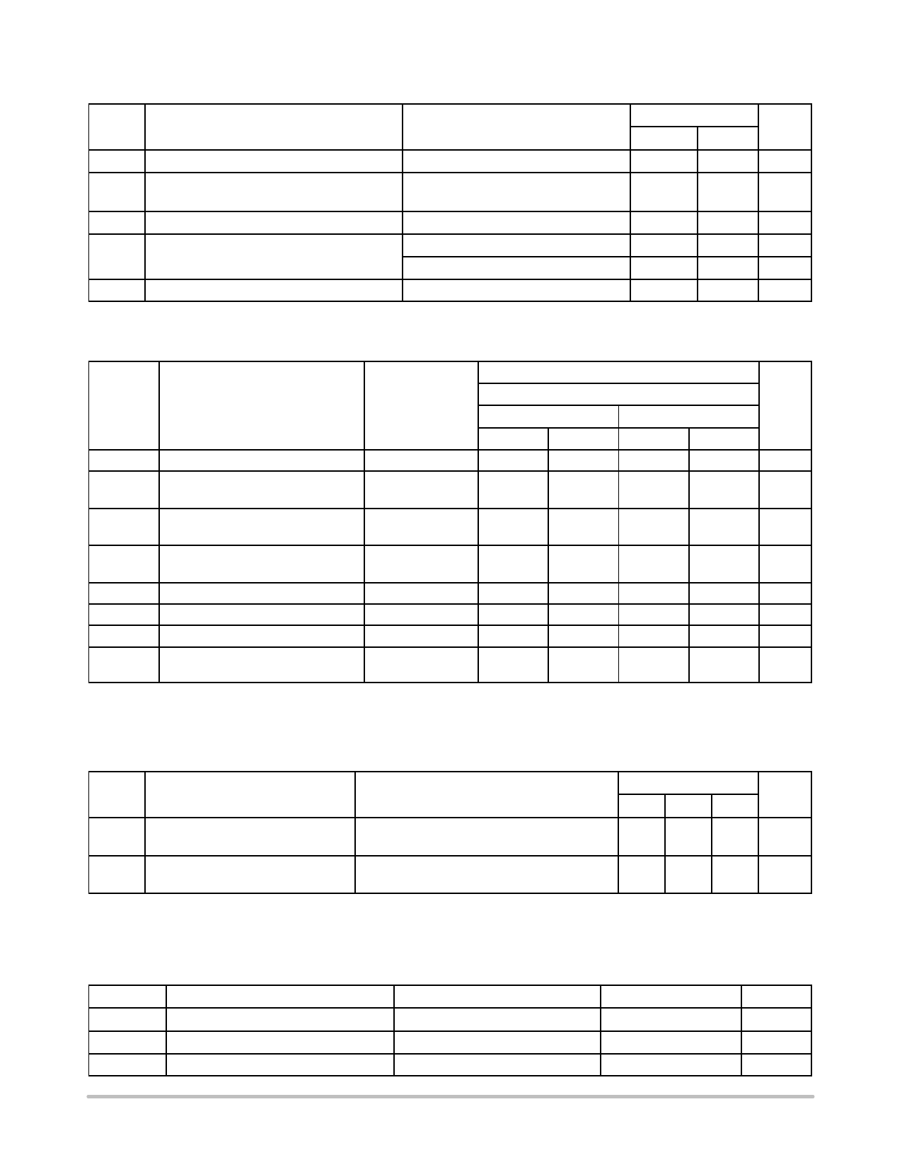
DC ELECTRICAL CHARACTERISTICS (continued)
Symbol
Characteristic
Condition
TA = –40°C to +85°C
Min
Max
Unit
II
Input Leakage Current
IOZ
3–State Output Current
2.7V ≤ VCC ≤ 3.6V; 0V ≤ VI ≤ 5.5V
2.7 ≤ VCC ≤ 3.6V; 0V ≤ VO ≤ 5.5V;
VI = VIH or V IL
±5.0
µA
±5.0
µA
IOFF
Power–Off Leakage Current
ICC
Quiescent Supply Current
∆ICC
Increase in ICC per Input
VCC = 0V; VI or VO = 5.5V
2.7 ≤ VCC ≤ 3.6V; VI = GND or VCC
2.7 ≤ VCC ≤ 3.6V; 3.6 ≤ VI or VO ≤ 5.5V
2.7 ≤ VCC ≤ 3.6V; VIH = VCC – 0.6V
10
µA
10
µA
±10
µA
500
µA
AC CHARACTERISTICS (tR = tF = 2.5ns; CL = 50pF; RL = 500Ω)
Limits
Symbol
Parameter
Waveform
TA = –40°C to +85°C
VCC = 3.0V to 3.6V
VCC = 2.7V
Min
Max
Min
Max
Unit
fmax
Clock Pulse Frequency
1
150
MHz
tPLH
Propagation Delay
tPHL
CP to On
1
1.5
8.5
1.5
9.5
ns
1.5
8.5
1.5
9.5
tPZH
Output Enable Time to HIGH and
2
1.5
8.5
1.5
9.5
ns
tPZL
LOW Levels
1.5
8.5
1.5
9.5
tPHZ
Output Disable Time from HIGH and
2
tPLZ
LOW Levels
1.5
7.5
1.5
8.5
ns
1.5
7.5
1.5
8.5
ts
Setup TIme, HIGH or LOW Dn to CP
1
2.5
2.5
ns
th
Hold TIme, HIGH or LOW Dn to CP
1
1.5
1.5
ns
tw
CP Pulse Width, HIGH or LOW
3
3.3
3.3
ns
tOSHL
tOSLH
Output–to–Output Skew
(Note 3.)
1.0
ns
1.0
3. Skew is defined as the absolute value of the difference between the actual propagation delay for any two separate outputs of the same device.
The specification applies to any outputs switching in the same direction, either HIGH–to–LOW (tOSHL) or LOW–to–HIGH (tOSLH); parameter
guaranteed by design.
DYNAMIC SWITCHING CHARACTERISTICS
Symbol
Characteristic
Condition
TA = +25°C
Min Typ Max Unit
VOLP
Dynamic LOW Peak Voltage (Note
VCC = 3.3V, CL = 50pF, VIH = 3.3V, VIL = 0V
0.8
V
4.)
VOLV
Dynamic LOW Valley Voltage (Note
VCC = 3.3V, CL = 50pF, VIH = 3.3V, VIL = 0V
0.8
V
4.)
4. Number of outputs defined as “n”. Measured with “n–1” outputs switching from HIGH–to–LOW or LOW–to–HIGH. The remaining output is
measured in the LOW state.
CAPACITIVE CHARACTERISTICS
Symbol
Parameter
Condition
Typical
Unit
CIN
Input Capacitance
VCC = 3.3V, VI = 0V or VCC
7
pF
COUT
Output Capacitance
VCC = 3.3V, VI = 0V or VCC
8
pF
CPD
Power Dissipation Capacitance
10MHz, VCC = 3.3V, VI = 0V or VCC
25
pF
http://onsemi.com
5
Share Link: 