74VCXH16245DT データシートの表示(PDF) - ON Semiconductor
部品番号
コンポーネント説明
メーカー
74VCXH16245DT
ON Semiconductor

74VCXH16245DT Datasheet PDF : 12 Pages
| |||
74VCXH16245
Low-Voltage 1.8/2.5/3.3V
16-Bit Transceiver
With 3.6 V–Tolerant Inputs and Outputs
(3–State, Non–Inverting)
The 74VCXH16245 is an advanced performance, non–inverting
16–bit transceiver. It is designed for very high–speed, very low–power
operation in 1.8 V, 2.5 V or 3.3 V systems.
When operating at 2.5 V (or 1.8 V) the part is designed to tolerate
voltages it may encounter on either inputs or outputs when interfacing
to 3.3 V busses. It is guaranteed to be over–voltage tolerant to 3.6 V.
The VCXH16245 is designed with byte control. It can be operated
as two separate octals, or with the controls tied together, as a 16–bit
wide function. The Transmit/Receive (T/Rn) inputs determine the
direction of data flow through the bi–directional transceiver. Transmit
(active–HIGH) enables data from A ports to B ports; Receive
(active–LOW) enables data from B to A ports. The Output Enable
inputs (OEn), when HIGH, disable both A and B ports by placing them
in a HIGH Z condition. The data inputs include active bushold
circuitry, eliminating the need for external pull–up resistors to hold
unused or floating inputs at a valid logic state.
http://onsemi.com
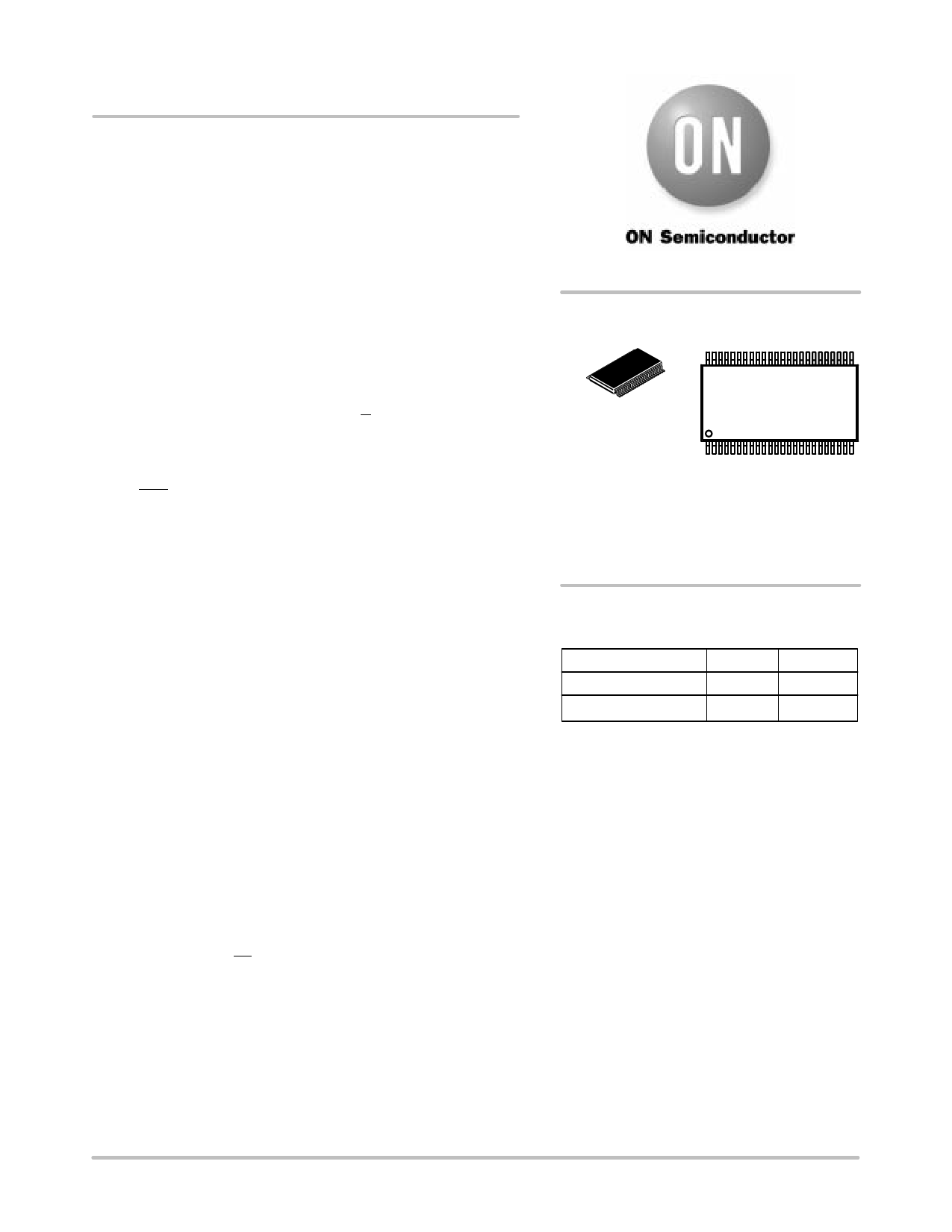
MARKING DIAGRAM
48
48
1
TSSOP–48
DT SUFFIX
CASE 1201
74VCXH16245DT
AWLYYWW
1
A = Assembly Location
WL = Wafer Lot
YY = Year
WW = Work Week
• Designed for Low Voltage Operation: VCC = 1.65–3.6 V
• 3.6 V Tolerant Inputs and Outputs
• High Speed Operation: 2.5 ns max for 3.0 to 3.6 V
3.0 ns max for 2.3 to 2.7 V
ORDERING INFORMATION
6.0 ns max for 1.65 to 1.95 V
Device
Package Shipping
• Static Drive: ±24 mA Drive at 3.0 V
74VCXH16245DT
TSSOP 39 / Rail
±18 mA Drive at 2.3 V
±6 mA Drive at 1.65 V
74VCXH16245DTR
TSSOP 2500 / Reel
• Supports Live Insertion and Withdrawal
• Includes Active Bushold to Hold Unused or Floating Inputs at a Valid
Logic State
• IOFF Specification Guarantees High Impedance When VCC = 0 V†
• Near Zero Static Supply Current in All Three Logic States (20 µA)
Substantially Reduces System Power Requirements
• Latchup Performance Exceeds ±250 mA @ 125°C
• ESD Performance: Human Body Model >2000 V; Machine Model >200 V
†NOTE: To ensure the outputs activate in the 3–state condition, the output
enable pins should be connected to VCC through a pull–up resistor. The
value of the resistor is determined by the current sinking capability of the
output connected to the OE pin.
© Semiconductor Components Industries, LLC, 2001
1
January, 2001 – Rev. 1
Publication Order Number:
74VCXH16245/D
Share Link: