ILC7082 データシートの表示(PDF) - Impala Linear Corporation
部品番号
コンポーネント説明
メーカー
ILC7082 Datasheet PDF : 16 Pages
| |||
150mA SOT-23 Ultra Low Noise CMOS RF-LDO™ Regulator
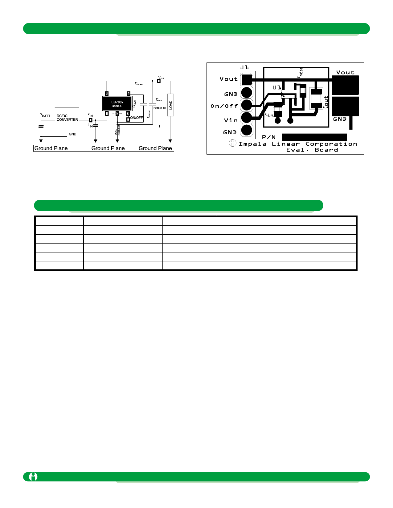
Figure 8: Recommended application circuit schematic.
Figure 9: Recommended application circuit layout ( not drawn to scale)
Note, ground plane is bottom layer of PCB and connects to top layer ground
connections through vias.
Evaluation Board Parts List For Printed Circuit Board Shown Above
Pin Number
U1
J1
Cin
Cnoise
Cout
Pin Name
ILC7082AIM5-30
69190-405
GRM40 Y5V 105Z16
ECU-V1H103KBV
GRM42-6X5R475K10
Manufacturer
Impala Linear
Berg
muRata
Panasonic
muRata
Description
150mA RF LDOTM regulator
Connector, four position header
Ceramic capacitor, 1µF,16V,SMT (size 0805)
Ceramic capacitor, 0.01µF,16V,SMT (size 0603)
Ceramic capacitor, 4.7µF16V,SMT (size 1206)
GROUNDING RECOMMENDATIONS
1. Connect CIN between VIN of the ILC7082 and the
“GROUND PLANE”.
2. Keep the ground side of COUT and CNOISE connected to the
“LOCAL GROUND” and not directly to the “GROUND PLANE”.
3. On multilayer boards use component side copper for
grounding around the ILC7082 and connect back to a
“GROUND PLANE” using vias.
4. If using a DC-DC converter in your design, use a star
grounding system with separate traces for the power
ground and the control signals. The star should radiate from
where the power supply enters the PCB.
LAYOUT CONSIDERATIONS
1. Place all RF LDO related components; ILC7082, input
capacitor CIN, noise bypass capacitor CNOISE and output
capacitor COUT as close together as possible.
2. Keep the output capacitor COUT as close to the ILC7082
as possible with very short traces to the VOUT and GND pins.
3. The traces for the related components; ILC7082, input
capacitor CIN, noise bypass capacitor CNOISE and output
capacitor COUT can be run with minimum trace widths close
to the LDO.
4. Maintain a separate “LOCAL GROUND” remote from the
“GROUND PLANE” to ensure a quiet ground near the LDO.
Figure 9 shows how this circuit can be translated into a
PCB layout.
Impala Linear Corporation
ILC7082 1.3
(408) 574-3939 www.impalalinear.com
April 1999 9
Share Link: 