CAT34WC02 データシートの表示(PDF) - Catalyst Semiconductor => Onsemi
部品番号
コンポーネント説明
メーカー
CAT34WC02 Datasheet PDF : 10 Pages
| |||
CAT34WC02
FUNCTIONAL DESCRIPTION
The CAT34WC02 supports the I2C Bus data transmis-
sion protocol. This Inter-Integrated Circuit Bus protocol
defines any device that sends data to the bus to be a
transmitter and any device receiving data to be a re-
ceiver. Data transfer is controlled by the Master device
which generates the serial clock and all START and
STOP conditions for bus access. The CAT34WC02
operates as a Slave device. Both the Master and Slave
devices can operate as either transmitter or receiver, but
the Master device controls which mode is activated. A
maximum of 8 devices may be connected to the bus as
determined by the device address inputs A0, A1, and A2.
PIN DESCRIPTIONS
SCL: Serial Clock
The CAT34WC02 serial clock input pin is used to clock
all data transfers into or out of the device. This is an input
pin.
SDA: Serial Data/Address
The CAT34WC02 bidirectional serial data/address pin
is used to transfer data into and out of the device. The
SDA pin is an open drain output and can be wire-ORed
with other open drain or open collector outputs.
A0, A1, A2: Device Address Inputs
These inputs set device address when cascading mul-
tiple devices. A maximum of eight devices can be
cascaded when using the device.
WP: Write Protect
This input, when tied to GND, allows write operations to
the entire memory. For CAT34WC02 when this pin is
tied to VCC, the entire array of memory is write protected.
When left floating, memory is unprotected.
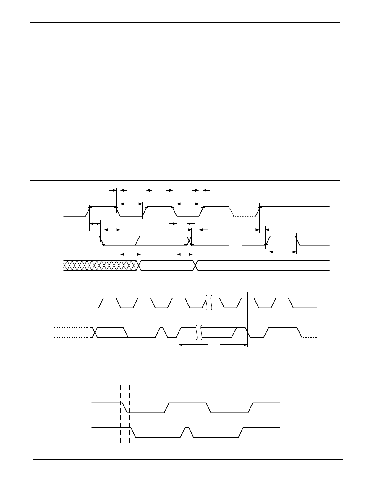
Figure 1. Bus Timing tF
SCL
tSU:STA
SDA IN
SDA OUT
tHIGH
tR
tLOW
tLOW
tHD:DAT
tHD:STA
tSU:DAT
tAA
tDH
tSU:STO
tBUF
5020 FHD F03
Figure 2. Write Cycle Timing
SCL
SDA
8TH BIT
BYTE n
ACK
Figure 3. Start/Stop Timing
SDA
SCL
Doc. No. 1003, Rev. A
START BIT
tWR
STOP
CONDITION
START
CONDITION
ADDRESS
5020 FHD F04
STOP BIT
4
5020 FHD F05
Share Link: 