CAT35C704 データシートの表示(PDF) - Catalyst Semiconductor => Onsemi
部品番号
コンポーネント説明
メーカー
CAT35C704 Datasheet PDF : 14 Pages
| |||
Preliminary
CAT35C704
also go to the high impedance state if an error condition
is detected. If the ENABLE BUSY instruction has not
been executed, to determine whether the device is in a
program/erase cycle or in an error condition, a READ
STATUS instruction may be entered. When the device
is in a program/erase cycle it will output an 8-bit status
word. If it does not, it is in an error condition.
PE
The Parity Enable pin is a TTL compatible input. If the PE
pin is set HIGH, the device will be configured to commu-
nicate using even parity, and if the pin is set LOW, it will
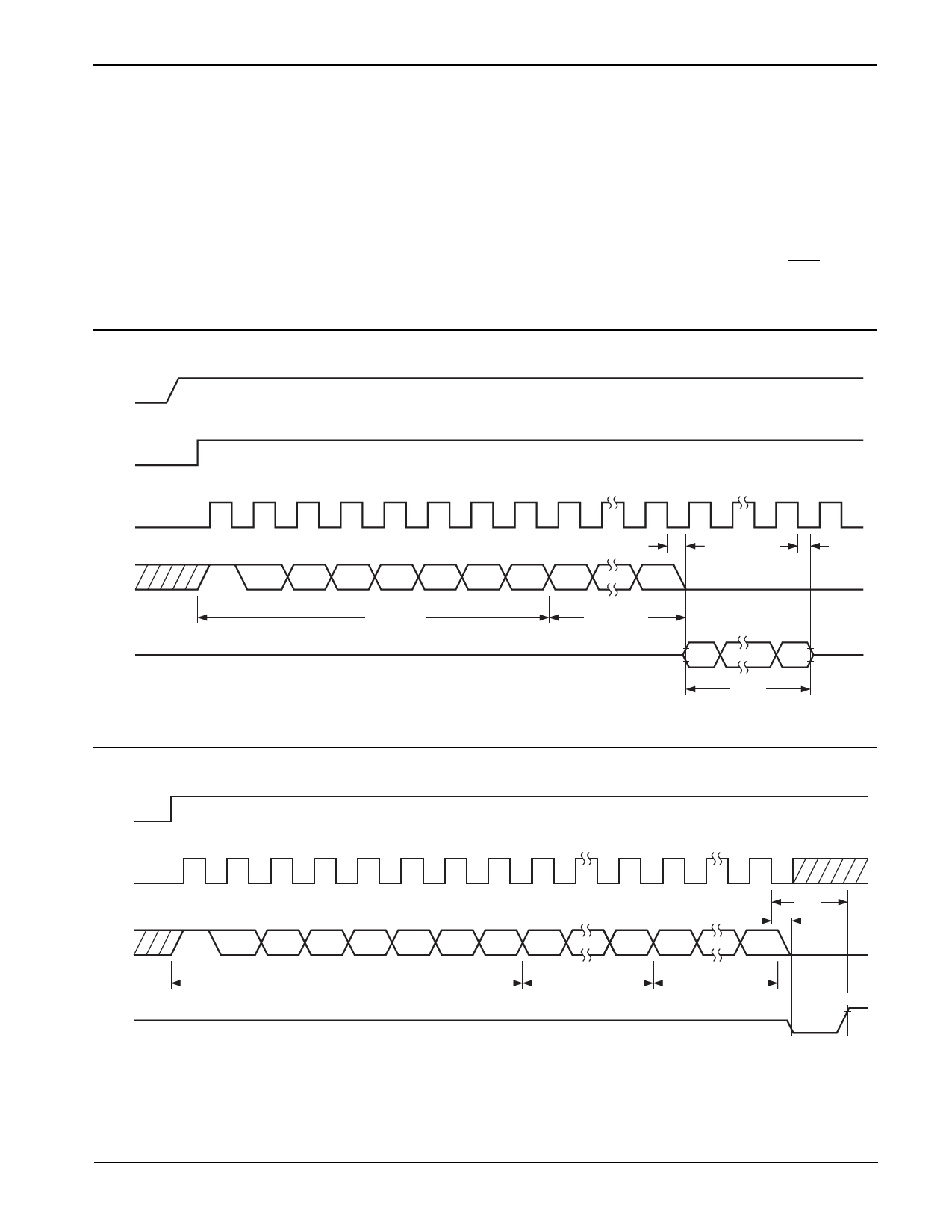
Figure 7. Read Timing
VCC
use no parity. In this case, instructions or data that
include parity bits will not be interpreted correctly. Note:
The PE input is internally pulled down to GND (i.e.
default = no parity). As with all CMOS devices, CS, CLK
and DI inputs must be connected to either HIGH or LOW,
and not left floating.
ERR
The Error indication pin is an open drain output. If either
an instruction or parity error exists, the ERR pin will
output a “0” until the device is reset. This can be done by
pulsing CS LOW.
CS
CLK
DI
OP7
DO
Figure 8. Write Timing
CS
CLK
DI
OP7
DO
OP CODE
HIGH-Z
tPD
tHZ
OP0 AN
A0
ADDRESS
DN
D0
DATA
5074 FHD F10
OP CODE
DON’T CARE
tEW
tSV
OP0
AN
A0
ADDRESS
DN
D0
DATA
READY
BUSY
5074 FHD F11
7
Doc. No. 25045-00 2/98
Share Link: 