CS5211GDR14G データシートの表示(PDF) - ON Semiconductor
部品番号
コンポーネント説明
メーカー
CS5211GDR14G Datasheet PDF : 13 Pages
| |||
CS5211
qSA is the sink−to−ambient thermal impedance of the
heatsink assuming direct mounting of the MOSFET (no
thermal “pad” is used).
TJ is the specified maximum allowed junction
temperature.
TA is the worst case ambient operating temperature.
For TO−220 and TO−263 packages, standard FR−4
copper clad circuit boards will have approximate thermal
resistances (qSA) as shown below:
Pad Size
(in2/mm2)
0.5/323
0.75/484
1.0/645
1.5/968
2.0/1290
2.5/1612
Single−Sided
1 oz. Copper
60−65°C/W
55−60°C/W
50−55°C/W
45−50°C/W
38−42°C/W
33−37°C/W
As with any power design, proper laboratory testing
should be performed to insure the design will dissipate the
required power under worst case operating conditions.
Variables considered during testing should include
maximum ambient temperature, minimum airflow,
maximum input voltage, maximum loading, and component
variations (i.e. worst case MOSFET RDS(on)). Also, the
inductors and capacitors share the MOSFET’s heatsinks and
will add heat and raise the temperature of the circuit board
and MOSFET. For any new design, its advisable to have as
much heatsink area as possible − all too often new designs
are found to be too hot and require re−design to add
heatsinking.
Compensation Capacitor Selection
The nominal output current capability of the error amp is
30 mA. This current charging the capacitor on the COMP pin
is used as soft−start for the converter. The COMP pin is going
to ramp up to a voltage level that is within 70 mV of what VFFB
is going to be when in regulation. This is the voltage that will
determine the soft−start. Therefore, the COMP capacitor can
be established by the following relationship:
C + 30 mA
soft start
VFFB(REG)
where:
soft−start = output ramp−up time
VFFB(REG) = VFFB voltage when in regulation
30 mA = COMP output current, typ.
The COMP output current range is given in the data sheet
and will affect the ramp−up time. The value of the capacitor on
the COMP pin will have an effect on the loop response and the
transient response of the converter. Transient response can be
enhanced by the addition of a parallel combination of a resistor
and capacitor between the COMP pin and the comp capacitor.
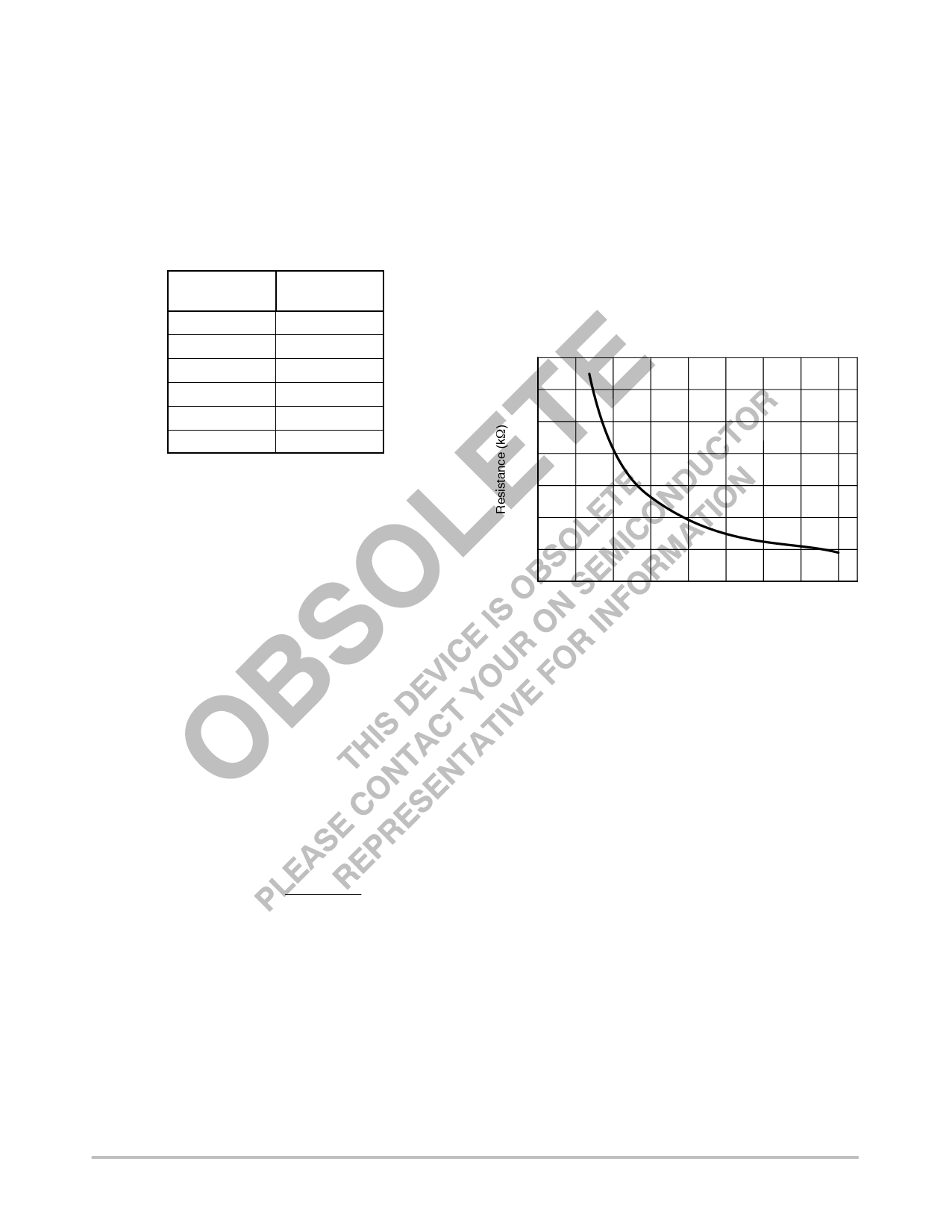
ROSC Selection
The switching frequency is programmed by selecting the
resistor connected between the ROSC pin and SGND (pin 7).
The grounded side of this resistor should be directly
connected to the SGND pin, without any other currents
flowing between the bottom of the resistor and the pin. Also,
avoid running any noisy signals under the resistor, since
injected noise could cause frequency jitter. The graph in
Figure 6 shows the required resistance to program the
frequency. Below 500 kHz, the following formula is
accurate:
R + 17544ńfSW * 4 kW
where fSW is the switching frequency in kHz.
140
120
100
80
60
40
20
0
0 100 200 300 400 500 600 700 800
Frequency (kHz)
Figure 6. Frequency vs. ROSC
Differential Remote Sense Operation
The ability to implement fully differential remote sense is
provided by the CS5211. The positive remote sense is
implemented by bringing the output remote sense connection
to the positive load connection. A low value resistor is
connected from Vout to the feedback point at the regulator to
provide feedback in the instance when the remote sense point
is not connected.
The negative remote sense connection is provided by
connecting the SGND of the CS5211 to the negative of the load
return. Again, a low value resistor should be connected
between SGND and LGND at the regulator to provide
feedback in the instance when the remote sense point is not
connected. The maximum voltage differential between the
three grounds for this part is 200 mV.
Feedback Divider Selection
The feedback voltage measured at VFB during normal
regulation will be 1.0 V. This voltage is compared to an internal
1.0 V reference and is used to regulate the output voltage. The
bias current into the error amplifier is 1.0 mA max, so select the
resistor values so that this current does not add an excessive
offset voltage.
http://onsemi.com
10
Share Link: 