CS5211EDR14G データシートの表示(PDF) - ON Semiconductor
部品番号
コンポーネント説明
メーカー
CS5211EDR14G Datasheet PDF : 13 Pages
| |||
CS5211
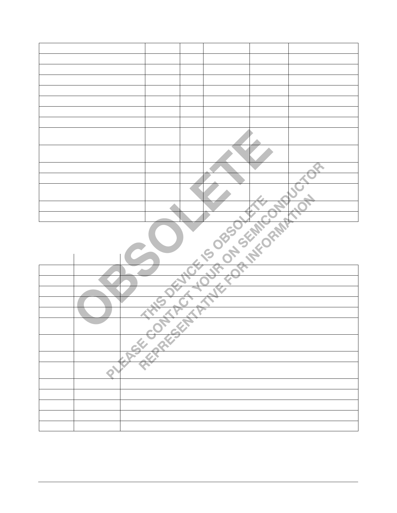
MAXIMUM RATINGS
Pin Name
IC Power Input
Power input for the low side driver
Power Supply input for the high side driver
Compensation Capacitor
Voltage Feedback Input
Oscillator Resistor
Fast Feedback Input
High−Side FET Driver
Pin Symbol
VCC
VC
BST
COMP
VFB
ROSC
VFFB
GATE(H)
VMAX
16 V
16 V
20 V
6.0 V
6.0 V
6.0 V
6.0 V
20 V
Low−Side FET Driver
GATE(L)
16 V
Positive Current Sense
Negative Current Sense
Power Ground
IS+
IS−
PGND
6.0 V
6.0 V
0.3 V
VMIN
−0.3 V
−0.3 V
−0.3 V
−0.3 V
−0.3 V
−0.3 V
−0.3 V
−0.3 V
−2.0 V for 50 ns
−0.3 V
−2.0 V for 50 ns
−0.3 V
−0.3 V
−0.3 V
Logic Ground
Sense Ground
LGND
SGND
0V
0.3 V
0V
−0.3 V
ISOURCE
N/A
N/A
N/A
1.0 mA
1.0 mA
1.0 mA
1.0 mA
1.5 A Peak
200 mA DC
1.5 A Peak,
200 mA DC
1.0 mA
1.0 mA
1.5 A Peak,
200 mA DC
100 mA
1.0 mA
ISINK
50 mA DC
1.5 A Peak, 200 mA DC
1.5 A Peak, 200 mA DC
1.0 mA
1.0 mA
1.0 mA
1.0 mA
1.5 A Peak, 200 mA DC
1.5 A Peak, 200 mA DC
1.0 mA
1.0 mA
N/A
N/A
1.0 mA
PACKAGE PIN DESCRIPTION
PIN NO.
1
PIN SYMBOL
GATE(H)
FUNCTION
High Side Switch FET driver pin. Capable of delivering peak currents of 1.0 A.
2
BST
Power supply input for the high side driver.
3
LGND
Reference ground. All control circuits are referenced to this pin. IC substrate connection.
4
VFFB
Input for the PWM comparator.
5
VFB
Error amplifier input.
6
COMP
Error Amp output. PWM Comparator reference input. A capacitor to LGND provides error amp
compensation.
7
SGND
Internal reference is connected to this ground. Connect directly at the load for ground remote
sensing.
8
ROSC
A resistor from this pin to SGND sets switching frequency.
9
VCC
Input Power Supply Pin. It supplies power to control circuitry. A 0.1 mF Decoupling cap is
recommended.
10
IS−
Negative input for overcurrent comparator.
11
IS+
Positive input for overcurrent comparator.
12
VC
Power supply input for the low side driver.
13
GATE(L)
Low Side Synchronous FET driver pin. Capable of delivering peak currents of 1.0 A.
14
PGND
High Current ground for the GATE(H) and GATE(L) pins.
http://onsemi.com
3
Share Link: 