CS5211GD14G データシートの表示(PDF) - ON Semiconductor
部品番号
コンポーネント説明
メーカー
CS5211GD14G Datasheet PDF : 13 Pages
| |||
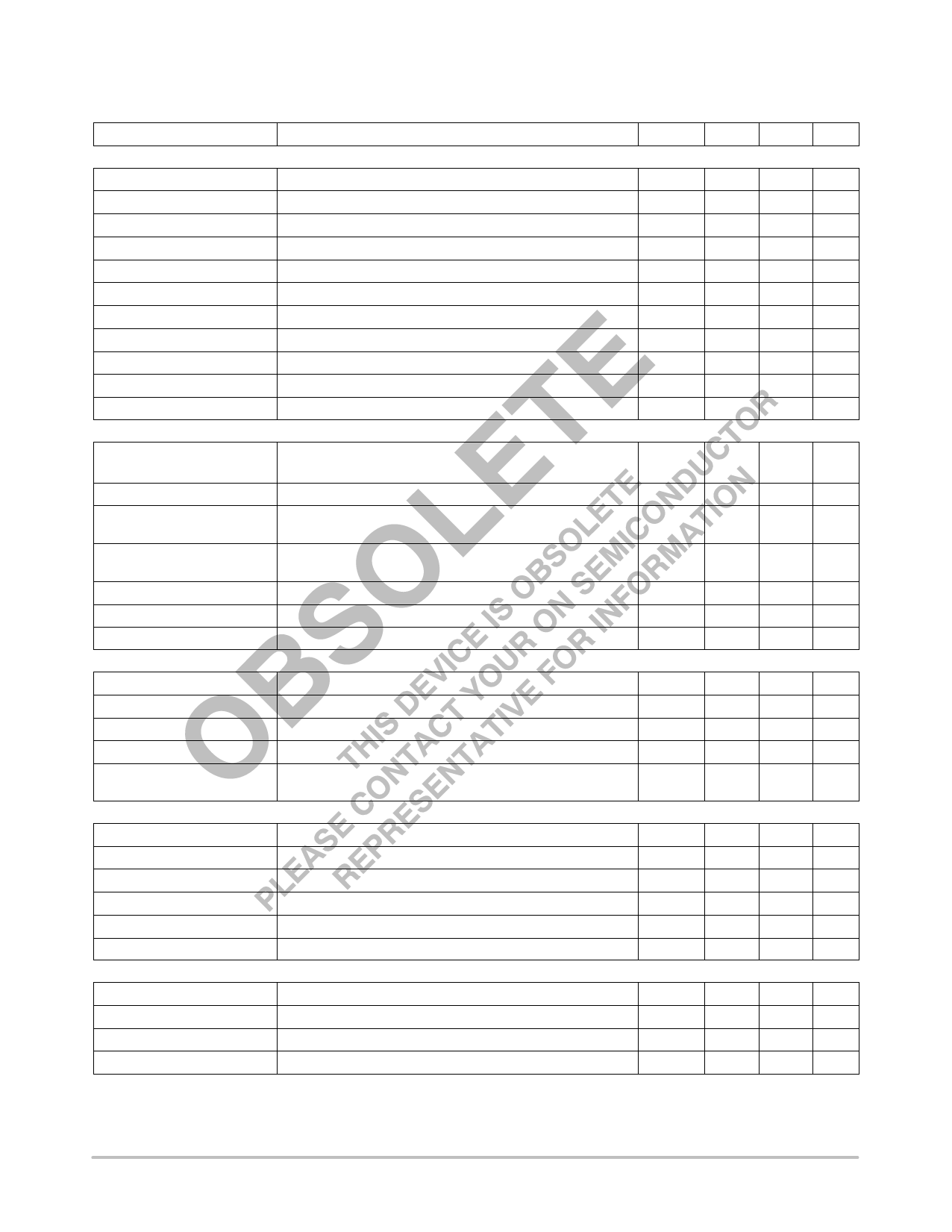
CS5211
ELECTRICAL CHARACTERISTICS (−40°C < TA < 85°C; −40°C < TJ < 125°C; 4.5 V < VCC, VC < 14 V; 7.0 V < BST < 20 V;
CGATE(H) = CGATE(L) = 3.3 nF; ROSC = 51 k; CCOMP = 0.1 mF, unless otherwise specified.) (Note 2)
Characteristic
Test Conditions
Min
Typ Max
Error Amplifier
VFB Bias Current
VFB = 0 V
COMP Source Current
VFB = 0.8 V
COMP SINK Current
VFB = 1.2 V
Open Loop Gain
−
−
0.1
1.0
15
30
60
15
30
60
−
98
−
Unity Gain Bandwidth
C = 0.1 mF
−
50
−
PSRR @ 1.0 kHz
−
−
70
−
Output Transconductance
−
−
32
−
Output Impedance
−
−
2.5
−
Reference Voltage
COMP Max Voltage
COMP Min Voltage
GATE(H) and GATE(L)
High Voltage (AC)
Low Voltage (AC)
Rise Time
−0.1 V < SGND < 0.1 V, COMP = VFB, Measure VFB to SGND
VFB = 0.8 V
VFB = 1.2 V
0.977
2.5
−
0.992
3.0
0.1
1.007
−
0.2
GATE(L),
GATE(H) 0.5 nF < CGATE(H) = CGATE(L) < 10 nF
GATE(L) or GATE(H) 0.5 nF < CGATE(H); CGATE(L) < 10 nF
VC = BST = 10 V, Measure:
1.0 V < GATE(L) < 9.0 V, 1.0 V < GATE(H) < 9.0 V
VC − 0.5
−
−
BST − 0.5
−
−
0.5
−
40
80
Fall Time
VC = BST = 10 V, Measure:
1.0 V < GATE(L) < 9.0 V, 1.0 V < GATE(H) < 9.0 V
−
40
80
GATE(H) to GATE(L) Delay
GATE(H) < 2.0 V, GATE(L) > 2.0 V
40
70
110
GATE(L) to GATE(H) Delay
GATE(L) < 2.0 V, GATE(H) > 2.0 V
40
70
110
GATE(H)/(L) Pull−Down
Resistance to PGND
20
50
115
Overcurrent Protection
OVC Comparator Offset Voltage
IS+ Bias Current
IS− Bias Current
COMP Discharge Threshold
0 V < IS+ < VCC, 0 V < IS− < VCC
0 V < IS+ < VCC
0 V < IS− < VCC
−
54
−1.0
−1.0
0.20
60
66
0.1
1.0
0.1
1.0
0.25 0.30
COMP Discharge Current in
OVC Fault Mode
COMP = 1.0 V
2.0
5.0
8.0
PWM Comparator
Transient Response
PWM Comparator Offset
Artificial Ramp
COMP = 0 − 1.5 V, VFFB, 20 mV overdrive
VFB = VFFB = 0 V; Increase COMP until GATE(H) starts switching
Duty Cycle = 90%
−
0.425
40
100
0.475
70
200
0.525
100
VFFB Bias Current
VFFB = 0 V
VFFB Input Range
(Note 4)
Minimum Pulse Width
−
−
0.1
1.0
−
−
1.1
−
−
200
Oscillator
Switching Frequency
ROSC = 18 k
Switching Frequency
ROSC = 51 k
Switching Frequency
ROSC = 115 kW
ROSC Voltage
−
2. Guaranteed by design. Not tested in production.
600
750
900
240
300
360
120
150
180
1.21
1.25 1.29
Unit
mA
mA
mA
dB
kHz
dB
mmho
MW
V
V
V
V
V
ns
ns
ns
ns
KW
mV
mA
mA
V
mA
ns
V
mV
mA
V
ns
kHz
kHz
kHz
V
http://onsemi.com
4
Share Link: 