CS5211EDR14 データシートの表示(PDF) - ON Semiconductor
部品番号
コンポーネント説明
メーカー
CS5211EDR14 Datasheet PDF : 13 Pages
| |||
CS5211
THEORY OF OPERATION
V2 Control Method
The V2 method of control uses a ramp signal that is
generated by the ESR of the output capacitors. This ramp is
proportional to the AC current through the main inductor
and is offset by the value of the DC output voltage. This
control scheme inherently compensates for variations in
either line or load conditions, since the ramp signal is
generated from the output voltage itself. This control
scheme differs from traditional techniques such as voltage
mode, which generates an artificial ramp, and current mode,
which generates a ramp from inductor current.
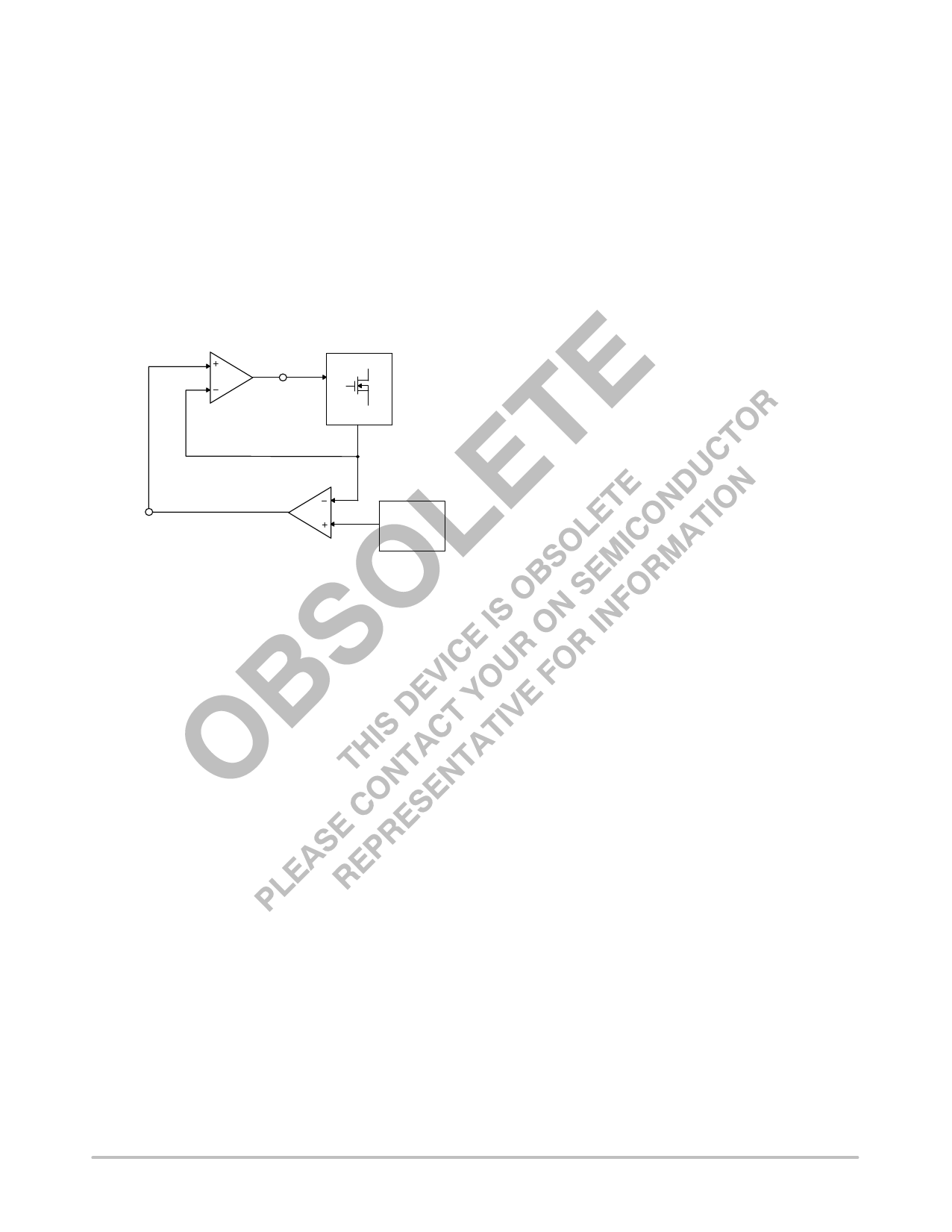
PWM Comparator
GATE(H)
GATE(L)
Ramp Signal
Error Amplifier
Output
Voltage
Feedback
COMP
Error Signal
Reference
Voltage
Figure 3. V2 Control Block Diagram
The V2 control method is illustrated in Figure 3. The
output voltage is used to generate both the error signal and
the ramp signal. Since the ramp signal is simply the output
voltage, it is affected by any change in the output regardless
of the origin of the change. The ramp signal also contains the
DC portion of the output voltage, which allows the control
circuit to drive the main switch to 0% or 100% duty cycle as
required.
A change in line voltage changes the current ramp in the
inductor, affecting the ramp signal, which causes the V2
control scheme to compensate the duty cycle. Since the
change in the inductor current modifies the ramp signal, as
in current mode control, the V2 control scheme has the same
advantages in line transient response.
A change in load current will have an effect on the output
voltage, altering the ramp signal. A load step immediately
changes the state of the comparator output, which controls
the main switch. Load transient response is determined only
by the comparator response time and the transition speed of
the main switch. The reaction time to an output load step has
no relation to the crossover frequency of the error signal
loop, as in traditional control methods.
The error signal loop can have a low crossover frequency,
since transient response is handled by the ramp signal loop.
The main purpose of this “slow” feedback loop is to provide
DC accuracy. Noise immunity is significantly improved,
since the error amplifier bandwidth can be rolled off at a low
frequency. Enhanced noise immunity improves remote
sensing of the output voltage, since the noise associated with
long feedback traces can be effectively filtered.
Line and load regulations are drastically improved
because there are two independent voltage loops. A voltage
mode controller relies on a change in the error signal to
compensate for a deviation in either line or load voltage.
This change in the error signal causes the output voltage to
change corresponding to the gain of the error amplifier,
which is normally specified as line and load regulation. A
current mode controller maintains fixed error signal under
deviation in the line voltage, since the slope of the ramp
signal changes, but still relies on a change in the error signal
for a deviation in load. The V2 method of control maintains
a fixed error signal for both line and load variations, since
both line and load affect the ramp signal.
Constant Frequency Operation
The CS5211 uses a constant frequency, trailing edge
modulation architecture for generating PWM signal. During
normal operation, the oscillator generates a narrow pulse at
the beginning of each switching cycle to turn on the main
switch. The main switch will be turned off when the ramp
signal intersects with the output of the error amplifier
(COMP pin voltage). Therefore, the switch duty cycle can
be modified to regulate the output voltage to the desired
value as line and load conditions change.
The major advantage of constant frequency operation is
that the component selections, especially the magnetic
component design, become very easy. The oscillator
frequency of CS5211 is programmable from 150 kHz to
750 kHz using an external resistor connected from the ROSC
pin to ground.
Startup
If there are no fault conditions and the fault latch is reset,
the error amplifier will start charging the COMP pin
capacitor after the CS5211 is powered up. The output of the
error amplifier (COMP voltage) will ramp up linearly. The
COMP capacitance and the source current of the error
amplifier determine the slew rate of COMP voltage. The
output of the error amplifier is connected internally to the
inverting input of the PWM comparator and it is compared
with the VFFB pin voltage plus 0.5 V offset at the
non−inverting input of the PWM comparator. Since VFFB
voltage is zero before the startup, the PWM comparator
output will stay high until the COMP pin voltage hits 0.5 V.
There is no switching action while the PWM comparator
output is high.
After the COMP voltage exceeds the 0.5 V offset, the
output of PWM comparator toggles and releases the PWM
latch. The narrow pulse generated by the oscillator at the
beginning of the next oscillator cycle will set the latch so that
the main switch can be turned on and the regulator output
voltage ramps up. When the output voltage achieves a level
set by the COMP voltage, the main switch will be turned off.
The V2 control loop will adjust the main switch duty cycle
as required to ensure the regulator output voltage tracks the
http://onsemi.com
6
Share Link: 