CS5211EDR14G データシートの表示(PDF) - ON Semiconductor
部品番号
コンポーネント説明
メーカー
CS5211EDR14G Datasheet PDF : 13 Pages
| |||
CS5211
the design must first predict the MOSFET power dissipation.
Once the dissipation is known, the heat sink thermal
impedance can be calculated to prevent the specified
maximum case or junction temperatures from being exceeded
at the highest ambient temperature. Power dissipation has two
primary contributors: conduction losses and switching losses.
The control or upper MOSFET will display both switching
and conduction losses. The synchronous or lower MOSFET
will exhibit only conduction losses because it switches into
nearly zero voltage. However, the body diode in the
synchronous MOSFET will suffer diode losses during the
non−overlap time of the gate drivers.
For the upper or control MOSFET, the power dissipation
can be approximated from:
PD,CONTROL + (IRMS,CNTL2 @ RDS(on))
) (ILo,MAX @ QswitchńIg @ VIN @ fSW)
) (Qossń2 @ VIN @ fSW) ) (VIN @ QRR @ fSW)
The first term represents the conduction or IR losses when
the MOSFET is ON while the second term represents the
switching losses. The third term is the losses associated with
the control and synchronous MOSFET output charge when
the control MOSFET turns ON. The output losses are caused
by both the control and synchronous MOSFET but are
dissipated only in the control FET. The fourth term is the loss
due to the reverse recovery time of the body diode in the
synchronous MOSFET. The first two terms are usually
adequate to predict the majority of the losses.
Where IRMS,CNTL is the RMS value of the trapezoidal
current in the control MOSFET:
IRMS,CNTL + ǸD @ [(ILo,MAX2 ) ILo,MAX @ ILo,MIN
) ILo,MIN2)ń3]1ń2
ILo,MAX is the maximum output inductor current:
ILo,MAX + IO,MAXń2 ) DILoń2
ILo,MIN is the minimum output inductor current:
ILo,MIN + IO,MAXń2 * DILoń2
IO,MAX is the maximum converter output current.
D is the duty cycle of the converter:
D + VOUTńVIN
DILo is the peak−to−peak ripple current in the output
inductor of value Lo:
DILo + (VIN * VOUT) @ Dń(Lo @ fSW)
RDS(on) is the ON resistance of the MOSFET at the
applied gate drive voltage.
Qswitch is the post gate threshold portion of the
gate−to−source charge plus the gate−to−drain charge. This
may be specified in the data sheet or approximated from the
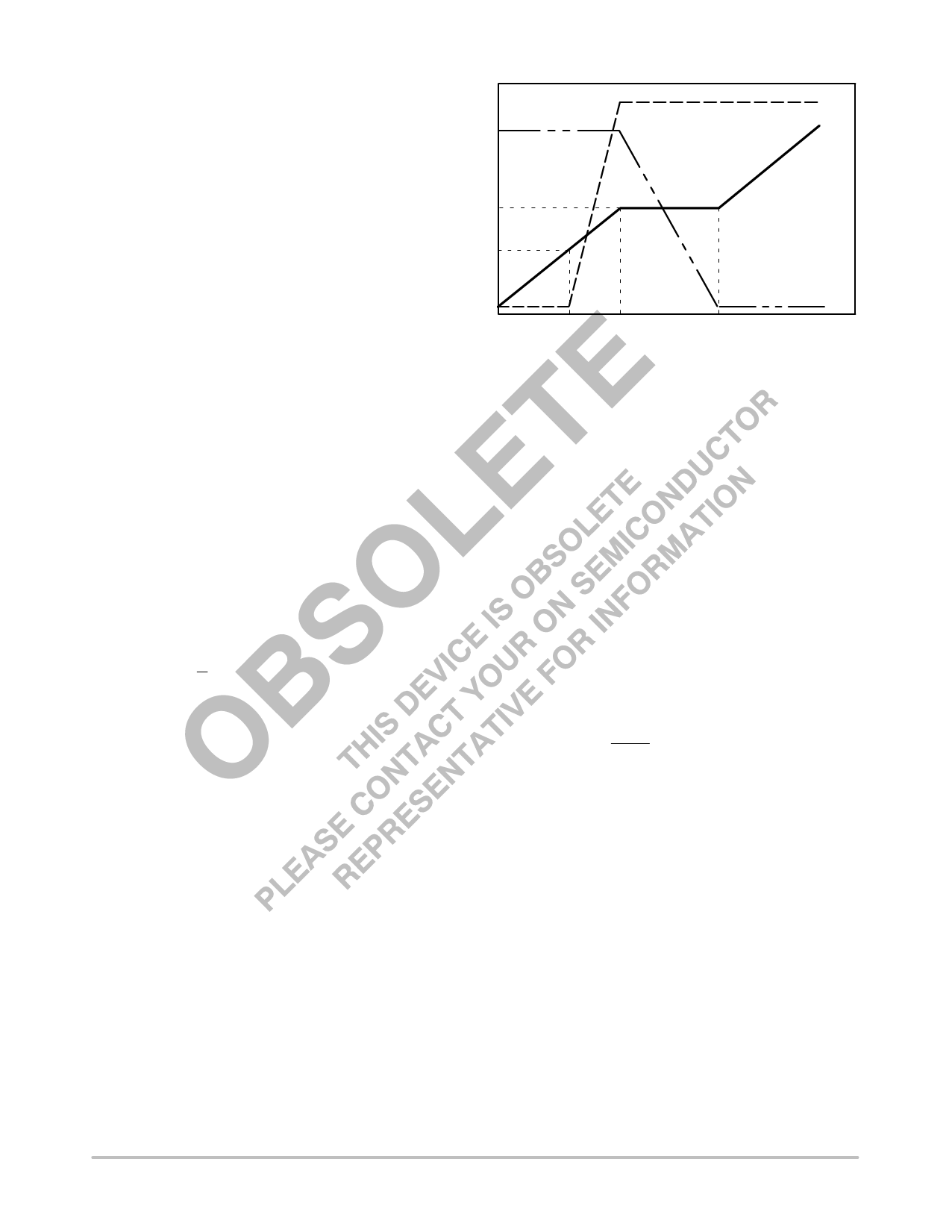
gate−charge curve as shown in the Figure 5.
Qswitch + Qgs2 ) Qgd
ID
VGATE
VGS_TH
QGS1 QGS2
QGD
VDRAIN
Figure 5. MOSFET Switching Characteristics
Ig is the output current from the gate driver IC.
VIN is the input voltage to the converter.
fsw is the switching frequency of the converter.
QG is the MOSFET total gate charge to obtain RDS(on).
Commonly specified in the data sheet.
Vg is the gate drive voltage.
QRR is the reverse recovery charge of the lower MOSFET.
Qoss is the MOSFET output charge specified in the data
sheet.
For the lower or synchronous MOSFET, the power
dissipation can be approximated from:
PD,SYNCH + (IRMS,SYNCH2 @ RDS(on))
) (Vfdiode @ IO,MAXń2 @ t_nonoverlap @ fSW)
The first term represents the conduction or IR losses when
the MOSFET is ON and the second term represents the diode
losses that occur during the gate non−overlap time.
All terms were defined in the previous discussion for the
control MOSFET with the exception of:
IRMS,SYNCH + Ǹ1 * D
@ [(ILo,MAX2 ) ILo,MAX @ ILo,MIN ) ILo,MIN2)ń3]1ń2
where:
Vfdiode is the forward voltage of the MOSFET’s intrinsic
diode at the converter output current.
t_nonoverlap is the non−overlap time between the upper
and lower gate drivers to prevent cross conduction. This
time is usually specified in the data sheet for the control
IC.
When the MOSFET power dissipations are known, the
designer can calculate the required thermal impedance to
maintain a specified junction temperature at the worst case
ambient operating temperature
qT t (TJ * TA)ńPD
where;
qT is the total thermal impedance (qJC + qSA).
qJC is the junction−to−case thermal impedance of the
MOSFET.
http://onsemi.com
9
Share Link: 