CS5203A-1 データシートの表示(PDF) - ON Semiconductor
部品番号
コンポーネント説明
メーカー
CS5203A-1 Datasheet PDF : 10 Pages
| |||
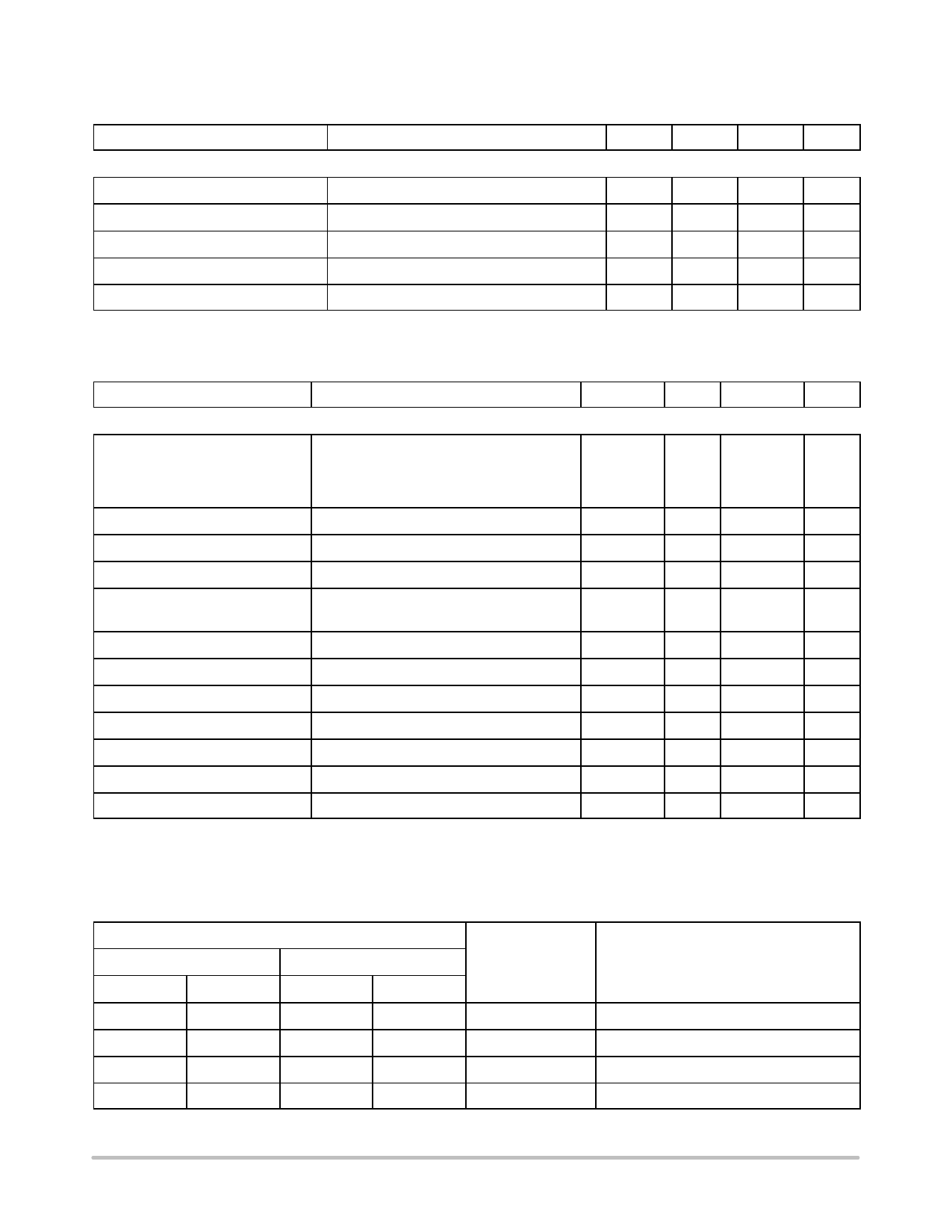
CS5203A−1, CS5203A−2, CS5203A−3, CS5203A−5
ELECTRICAL CHARACTERISTICS (continued) (CIN = 10 mF, COUT = 22 mF Tantalum, VIN − VOUT = 3.0 V, VIN ≤ 15 V,
0°C ≤ TA ≤ 70°C, TJ ≤ +150°C, unless otherwise specified, Ifull load = 3.0 A.)
Characteristic
Test Conditions
Min
Typ
Max
Adjustable Output Voltage (CS5203A−1) (continued)
Ripple Rejection
Temperature Stability
f = 120 Hz; CAdj = 25 mF; IOUT = 3.0 A
−
−
85
−
−
0.5
−
RMS Output Noise
Thermal Shutdown
10 Hz ≤ f ≤ 10 kHz; TA = 25°C
−
−
0.003
−
150
180
−
Thermal Shutdown Hysteresis
−
−
25
−
Unit
dB
%
%VOUT
°C
°C
ELECTRICAL CHARACTERISTICS (CIN = 10 mF, COUT = 22 mF Tantalum, VIN − VOUT = 3.0 V, VIN ≤ 15 V,
0°C ≤ TA ≤ 70°C, TJ ≤ +150°C, unless otherwise specified, Ifull load = 3.0 A.)
Characteristic
Test Conditions
Min
Typ
Max
Unit
Fixed Output Voltage (CS5203A−2, CS5203A−3, CS5203A−5)
Reference Voltage (Notes 6 and 7)
CS5203A−5
CS5203A−3
CS5203A−2
Line Regulation
Load Regulation (Notes 6 and 7)
Dropout Voltage (Note 8)
Current Limit
Quiescent Current
Thermal Regulation
Ripple Rejection
Temperature Stability
VIN − VOUT = 1.5 V; 0 ≤ IOUT ≤ 3.0A
VIN − VOUT = 1.5 V; 0 ≤ IOUT ≤ 3.0A
VIN − VOUT = 1.5 V; 0 ≤ IOUT ≤ 3.0A
1.5 V ≤ VIN − VOUT ≤ 6.0 V; IOUT = 10 mA
VIN − VOUT = 1.5 V; 10 mA ≤ IOUT ≤ 3.0 A
IOUT = 3.0 A
VIN − VOUT = 3.0 V; TJ ≥ 25°C
VIN − VOUT = 15 V
VIN ≤ 9.0 V; IOUT = 10 mA
30 ms pulse; TA = 25°C
f = 120 Hz; IOUT = 3.0 A
−
4.9 (−2%)
5.0
3.234 (−2%) 3.3
1.47 (−2%) 1.5
−
0.04
−
0.03
−
1.05
3.2
5.5
−
2.5
−
5.0
−
0.003
−
78
−
0.5
5.1 (+2%)
3.366 (+2%)
1.53 (+2%)
0.20
0.4
1.15
−
−
10
−
−
−
V
V
V
%
%
V
A
A
mA
%/W
dB
%
RMS Output Noise (%VOUT)
Thermal Shutdown
10 Hz ≤ f ≤ 10 kHz
−
−
0.003
150
180
−
%VOUT
−
°C
Thermal Shutdown Hysteresis
−
−
25
−
°C
6. Load regulation and output voltage are measured at a constant junction temperature by low duty cycle pulse testing. Changes in output
voltage due to thermal gradients or temperature changes must be taken into account separately.
7. Specifications apply for an external Kelvin sense connection at a point on the output pin 1/4” from the bottom of the package.
8. Dropout voltage is a measurement of the minimum input/output differential at full load.
PACKAGE PIN DESCRIPTION
Package Pin Number
CS5203A−1
D2PAK−3
TO−220−3
CS5203A−2, −3, −5
D2PAK−3
TO−220−3
1
1
N/A
N/A
2
2
2
2
3
3
3
3
N/A
N/A
1
1
Pin Symbol
Adj
VOUT
VIN
GND
Function
Adjust pin (low side of the internal reference).
Regulated output voltage (case).
Input voltage.
Ground connection.
http://onsemi.com
3
Share Link: 