CS5203A-1 データシートの表示(PDF) - ON Semiconductor
部品番号
コンポーネント説明
メーカー
CS5203A-1 Datasheet PDF : 10 Pages
| |||
CS5203A−1, CS5203A−2, CS5203A−3, CS5203A−5
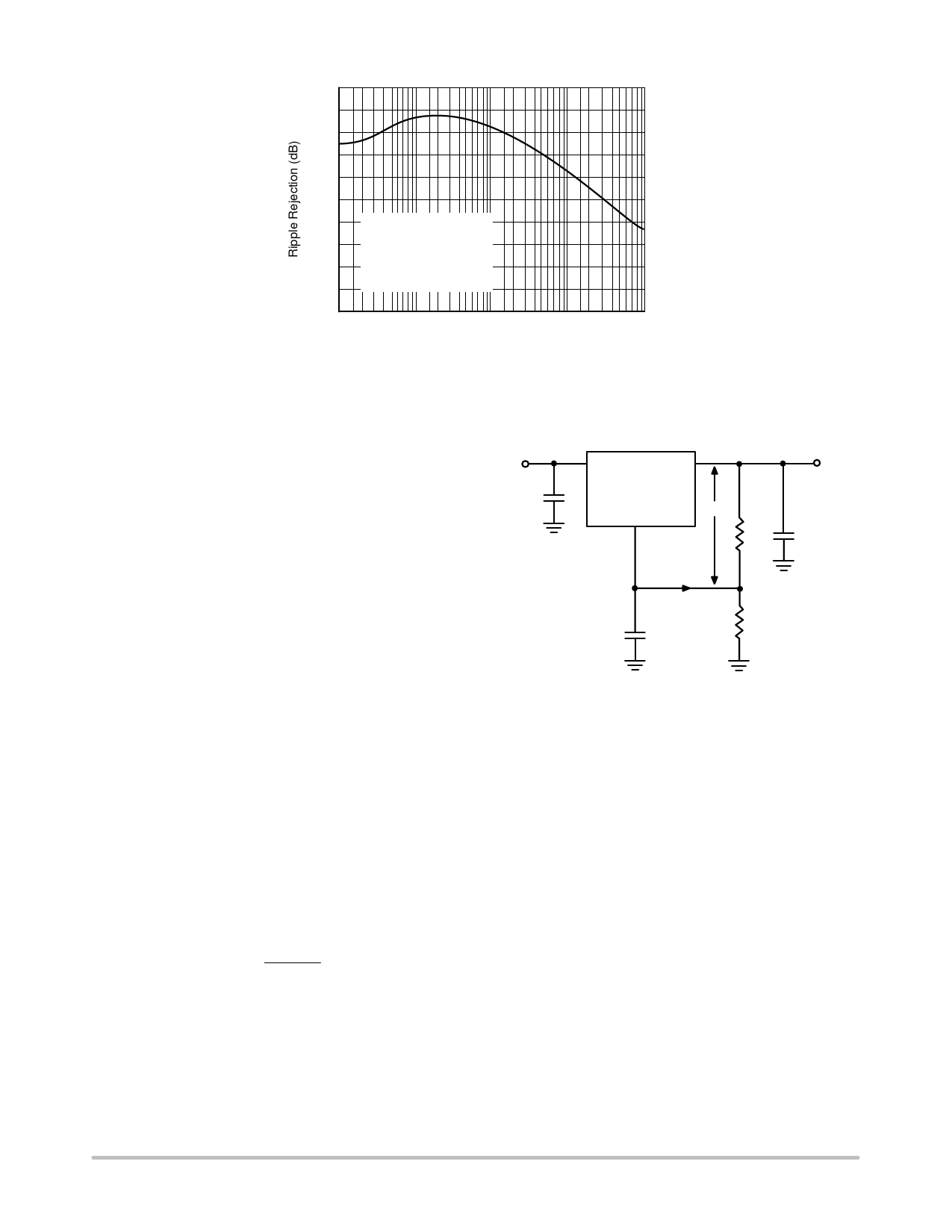
100
90
80
70
60
50
40
TCASE = 25°C
30
IOUT = 3.0 A
(VIN − VOUT) = 3.0 V
20
VRIPPLE = 1.6 VPP
10
CAdj = 25 mF
0
101
102
103
104
105
Frequency (Hz)
Figure 9. Ripple Rejection vs. Frequency
(Adjustable Versions)
APPLICATIONS INFORMATION
The CS5203A family of linear regulators provides fixed
or adjustable voltages at currents up to 3.0 A. The regulators
are protected against short circuit, and include thermal
shutdown and safe area protection (SOA) circuitry. The
SOA protection circuitry decreases the maximum available
output current as the input−output differential voltage
increases.
The CS5203A has a composite PNP−NPN output
transistor and requires an output capacitor for stability. A
detailed procedure for selecting this capacitor is included in
the Stability Considerations section.
VIN
C1
VIN
VOUT
CS5203A−1
Adj
VREF
R1
VOUT
C2
IAdj
R2
CAdj
Adjustable Operation
The adjustable regulator (CS5203A−1) has an output
voltage range of 1.25 V to 13 V. An external resistor divider
sets the output voltage as shown in Figure 10. The regulator
maintains a fixed 1.25 V (typical) reference between the
output pin and the adjust pin.
A resistor divider network R1 and R2 causes a fixed
current to flow to ground. This current creates a voltage
across R2 that adds to the 1.25 V across R1 and sets the
overall output voltage. The adjust pin current (typically
50 mA) also flows through R2 and adds a small error that
should be taken into account if precise adjustment of VOUT
is necessary.
The output voltage is set according to the formula:
ǒ Ǔ VOUT + VREF
R1 ) R2
R1
) IAdj
R2
The term IAdj × R2 represents the error added by the adjust
pin current.
R1 is chosen so that the minimum load current is at least
10 mA. R1 and R2 should be the same type, e.g. metal film
for best tracking over temperature. The adjust pin is
bypassed to improve the transient response and ripple
rejection of the regulator.
Figure 10. Resistor Divider Scheme for the
Adjustable Version
Stability Considerations
The output or compensation capacitor helps determine
three main characteristics of a linear regulator: satrtup delay,
load transient response and loop stability.
The capacitor value and type is based on cost, availability,
size and temperature constraints. A tantalum or aluminum
electrolytic capacitor is best, since a film or ceramic
capacitor with almost zero ESR, can cause instability. The
aluminum electrolytic capacitor is the least expensive
solution. However, when the circuit operates at low
temperatures, both the value and ESR of the capacitor will
vary considerably. The capacitor manufacturers data sheet
provides this information.
A 22 mF tantalum capacitor will work for most
applications, but with high current regulators such as the
CS5203A the transient response and stability improve with
higher values of capacitor. The majority of applications for
this regulator involve large changes in load current so the
output capacitor must supply the instantaneous load current.
http://onsemi.com
5
Share Link: 