MB89965 データシートの表示(PDF) - Fujitsu
部品番号
コンポーネント説明
メーカー
MB89965 Datasheet PDF : 48 Pages
| |||
MB89960 Series
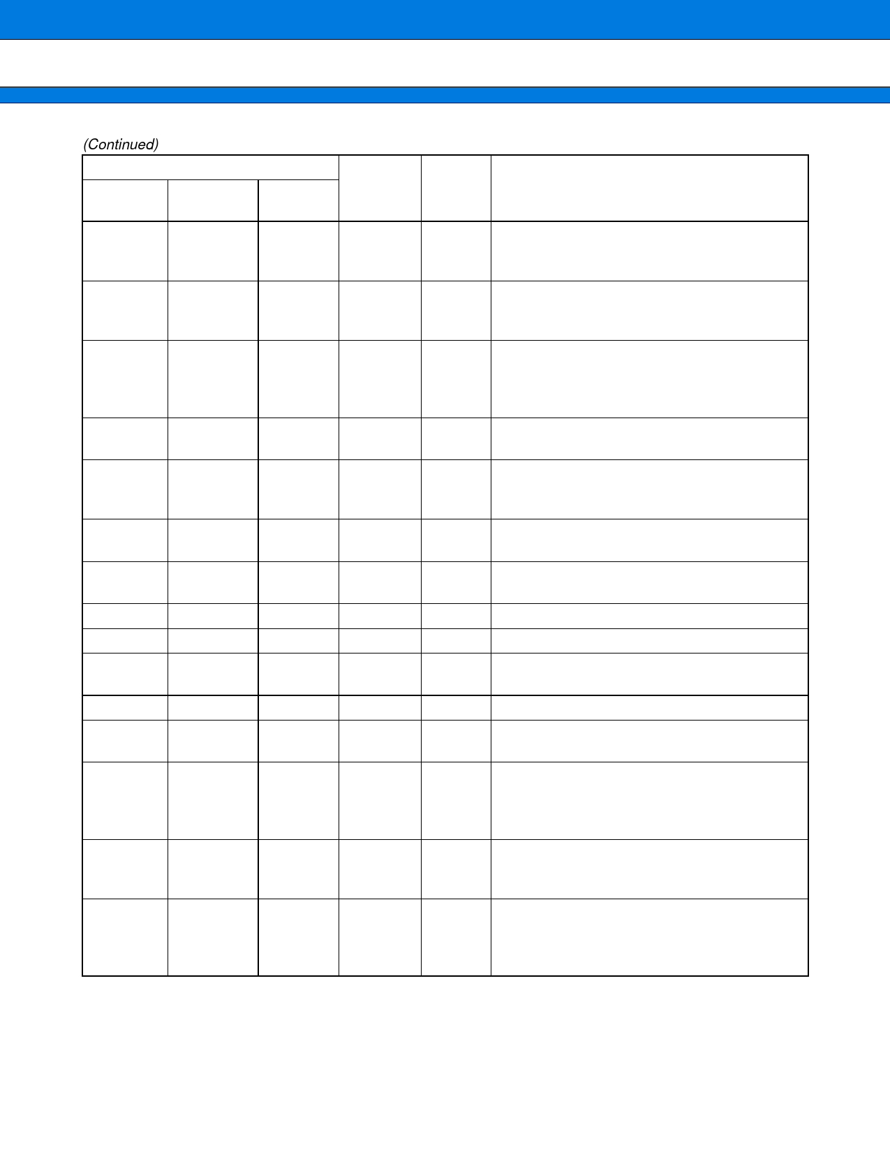
(Continued)
MQFP-48*3
Pin No.
LQFP-48*1
QFP-48*2
Pin Name
LQFP-64*4
38
38
52
P32/SI
37
37
51
P33/EC
36
36
46
P34/TO/
CLK
45 to 48
42
41
7
19
1
44
43
35
35
45 to 48
42
41
7
19
1
44
43
45
59 to 62
56
C
P40/AN0
to
P43/AN3
P44/SDA
55
9
25
3
58
57
15 to 18
31 to 34
47 to 50
63, 64
P45/SCL
VCC
VSS
AVCC
AVR
AVSS
N.C.
1
TEST
2
*1 : FPT-48P-M05
*2 : FPT-48P-M16, FPT-48P-M13
*3 : MQP-48C-P01
*4 : FPT-64P-M09
MOD2
Circuit
Type
Function
General-purpose I/O port
F Also serves as the serial I/O data input.
A hysteresis input.
General-purpose I/O port
F Also serves as the external clock input for the 8/
16-bit timer/counter. A hysteresis input.
General-purpose I/O port
F
Also serves as the overflow output for the 8/16-
bit timer/counter and the CLK clock
output. A hysteresis input.
Connect a 0.1 µF capacitor on the MB89965,
MB89P965A, and MB89F969A.
H
General-purpose Nch open-drain outputs.
Also serves as the A/D converter analog inputs.
I
General-purpose Nch open-drain output.
Also serves as the I2C interface data output.
I
General-purpose Nch open-drain output.
Also serves as the I2C interface clock I/O.
Power supply pin
Power supply (GND) pin
A/D converter power supply pin
Use this pin at the same voltage as VCC.
A/D converter reference voltage input pin
A/D converter power supply pin
Use this pin at the same voltage as VSS.
These pins are not connected.
Do not connect these on the MB89PV960.
TEST pin. Connect directly to VSS.
C Only used on the MB89F969A.
Treat as an N.C. pin on the MB89965.
Memory access mode setting pin. Connect di-
C
rectly to VSS.
Only used on the MB89F969A.
Treat as an N.C. pin on the MB89965.
10
Share Link: 