EVB71101 データシートの表示(PDF) - Melexis Microelectronic Systems
部品番号
コンポーネント説明
メーカー
EVB71101 Datasheet PDF : 14 Pages
| |||
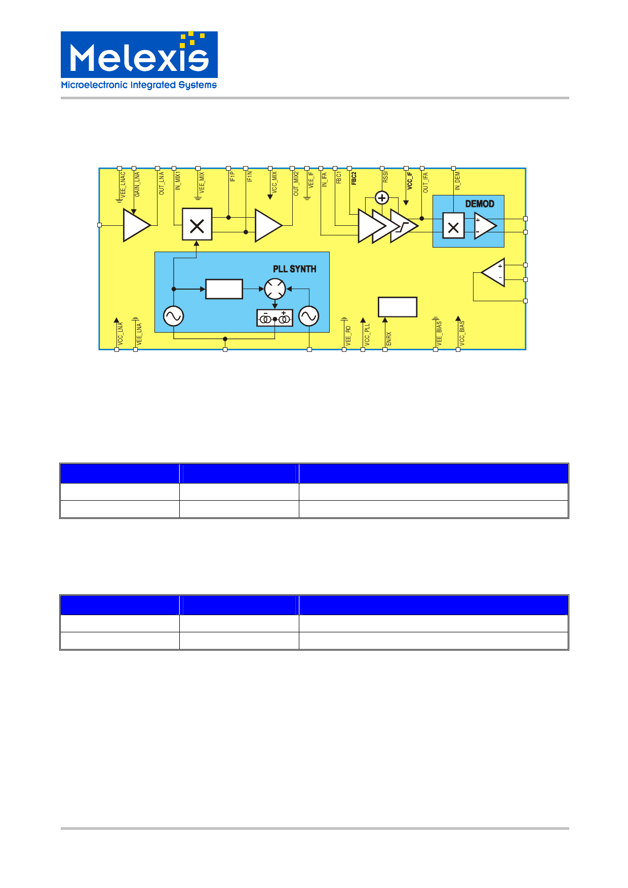
1.3 Block Diagram
EVB71101
315/433MHz Receiver
Evaluation Board Description
12
34
5
6
7
8
9 10 11 12 13
21
14 15
16
IN_LNA
31
LNA
32 30
MIX1
IF
MIX2
IF
IFA
LO
MIX3
DIV_16
PFD
RO
VCO1
CP
BIAS
29 LF
26 RO
25 27
28
Fig. 1: TH71101 block diagram
22
17
OUTP
23
OUTN
24
OAP
OA
20
OAN
19
OUT_OA
18
1.4 Mode Configurations
ENRX
Mode
0
RX standby
1
RX active
Note: ENRX are pulled down internally
Description
RX disabled
RX enable
1.5 LNA GAIN Control
VGAIN_LNA
< 0.8 V
Mode
HIGH GAIN
> 1.4 V
LOW GAIN
Note: hysteresis between gain modes to ensure stability
Description
LNA set to high gain
LNA set to low gain
1.6 Frequency Planning
Frequency planning is straightforward for single-conversion applications because there is only one IF that
can be chosen, and then the only possible choice is low-side or high-side injection of the LO signal (which is
now the one and only LO signal in the receiver).
The receiver’s single-conversion architecture requires careful frequency planning. Besides the desired RF
input signal, there are a number of spurious signals that may cause an undesired response at the output.
Among them is the image of the RF signal that must be suppressed by the RF front-end filter.
39012 71101 01
Rev. 011
Page 4 of 14
EVB Description
June/07
Share Link: 