HT48R70A-1 データシートの表示(PDF) - Holtek Semiconductor
部品番号
コンポーネント説明
メーカー
HT48R70A-1 Datasheet PDF : 39 Pages
| |||
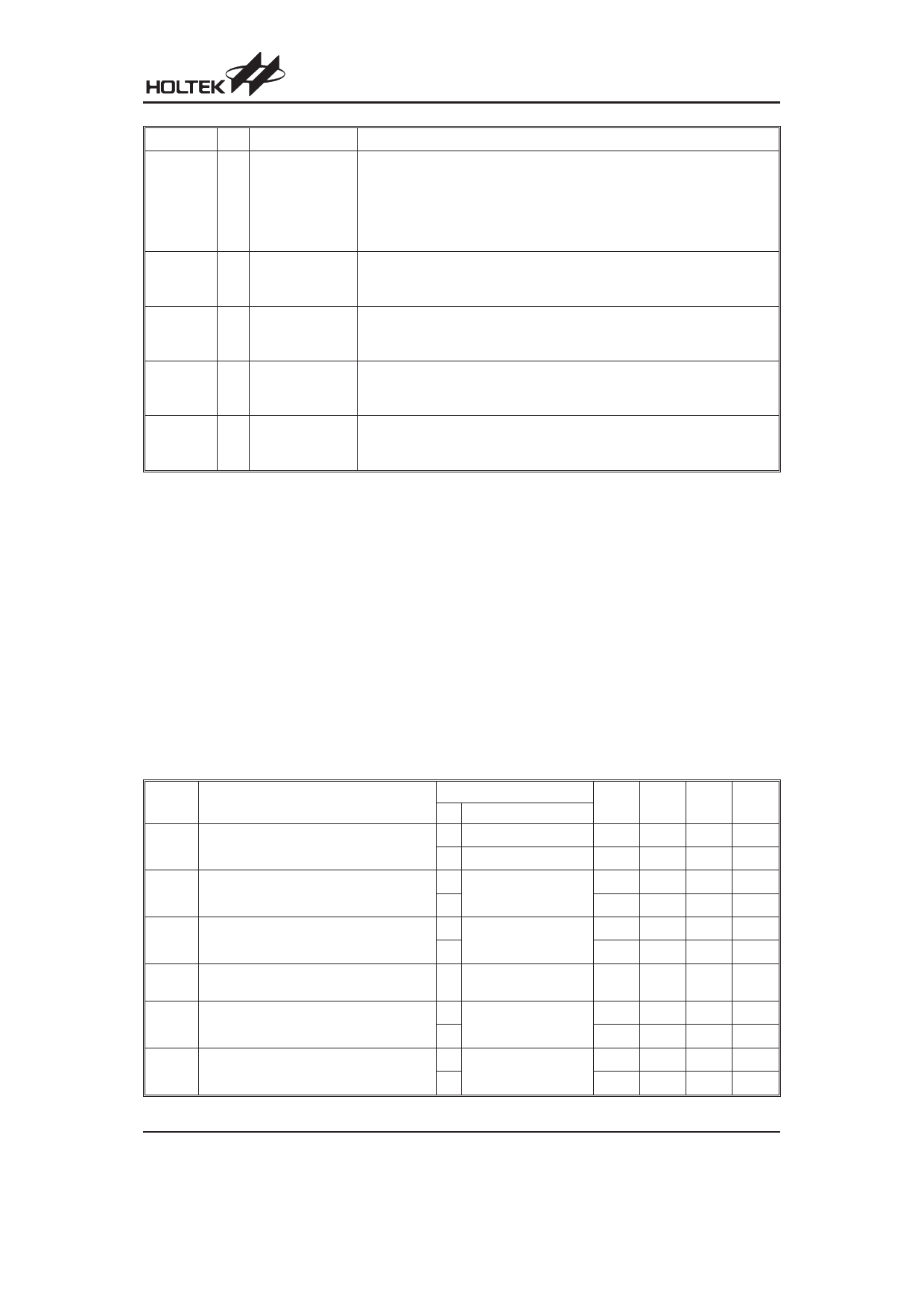
HT48R70A-1/HT48C70-1
Pin Name I/O
Options
Description
OSC1 and OSC2 are connected to an RC network or a crystal (by options) for
OSC1
OSC2
I
O
Crystal
or RC
or RTC
the internal system clock. In the case of RC operation, OSC2 is the output
terminal for 1/4 system clock.
These two pins also can be optioned as an RTC oscillator (32768Hz). In this
case, the system clock comes from an internal RC oscillator whose fre-
quency has 4 options (3.2MHz, 1.6MHz, 800kHz, 400kHz)
PD0~PD7 I/O
Pull-high*
Bidirectional 8-bit input/output ports
Software instructions determine the CMOS output or Schmitt trigger input
(pull-high depends on options).
PE0~PE7 I/O
Pull-high*
Bidirectional 8-bit input/output ports
Software instructions determine the CMOS output or Schmitt trigger input
(pull-high depends on options).
PF0~PF7 I/O
Pull-high*
Bidirectional 8-bit input/output ports
Software instructions determine the CMOS output or Schmitt trigger input
(pull-high depends on options).
PG0~PG7 I/O
Pull-high*
Bidirectional 8-bit input/output ports
Software instructions determine the CMOS output or Schmitt trigger input
(pull-high depends on options).
Note: * The pull-high resistors of each I/O port (PA, PB, PC, PD, PE, PF, PG) are controlled by an option.
CMOS or Schmitt trigger option of port A is controlled by an option.
Absolute Maximum Ratings
Supply Voltage ...........................VSS-0.3V to VSS+6.0V
Input Voltage..............................VSS-0.3V to VDD+0.3V
IOL Total ..............................................................150mA
Total Power Dissipation .....................................500mW
Storage Temperature ............................-50°C to 125°C
Operating Temperature...........................-40°C to 85°C
IOH Total............................................................-100mA
Note: These are stress ratings only. Stresses exceeding the range specified under ²Absolute Maximum Ratings² may
cause substantial damage to the device. Functional operation of this device at other conditions beyond those
listed in the specification is not implied and prolonged exposure to extreme conditions may affect device reliabil-
ity.
D.C. Characteristics
Symbol
Parameter
Test Conditions
VDD
Conditions
Min.
VDD
Operating Voltage
¾ fSYS=4MHz
2.2
¾ fSYS=8MHz
3.3
IDD1
Operating Current (Crystal OSC)
3V
¾
No load, fSYS=4MHz
5V
¾
IDD2
Operating Current (RC OSC)
3V
¾
No load, fSYS=4MHz
5V
¾
IDD3
Operating Current
(Crystal OSC, RC OSC)
5V No load, fSYS=8MHz
¾
ISTB1
3V
¾
Standby Current (WDT Enabled RTC Off)
No load, system HALT
5V
¾
ISTB2
3V
¾
Standby Current (WDT Disabled RTC Off)
No load, system HALT
5V
¾
Typ.
¾
¾
0.6
2
0.8
2.5
4
¾
¾
¾
¾
Ta=25°C
Max. Unit
5.5
V
5.5
V
1.5 mA
4
mA
1.5 mA
4
mA
8
mA
5
mA
10
mA
1
mA
2
mA
Rev. 2.10
4
August 7, 2007
Share Link: 