HV232 データシートの表示(PDF) - Supertex Inc
部品番号
コンポーネント説明
メーカー
HV232 Datasheet PDF : 11 Pages
| |||
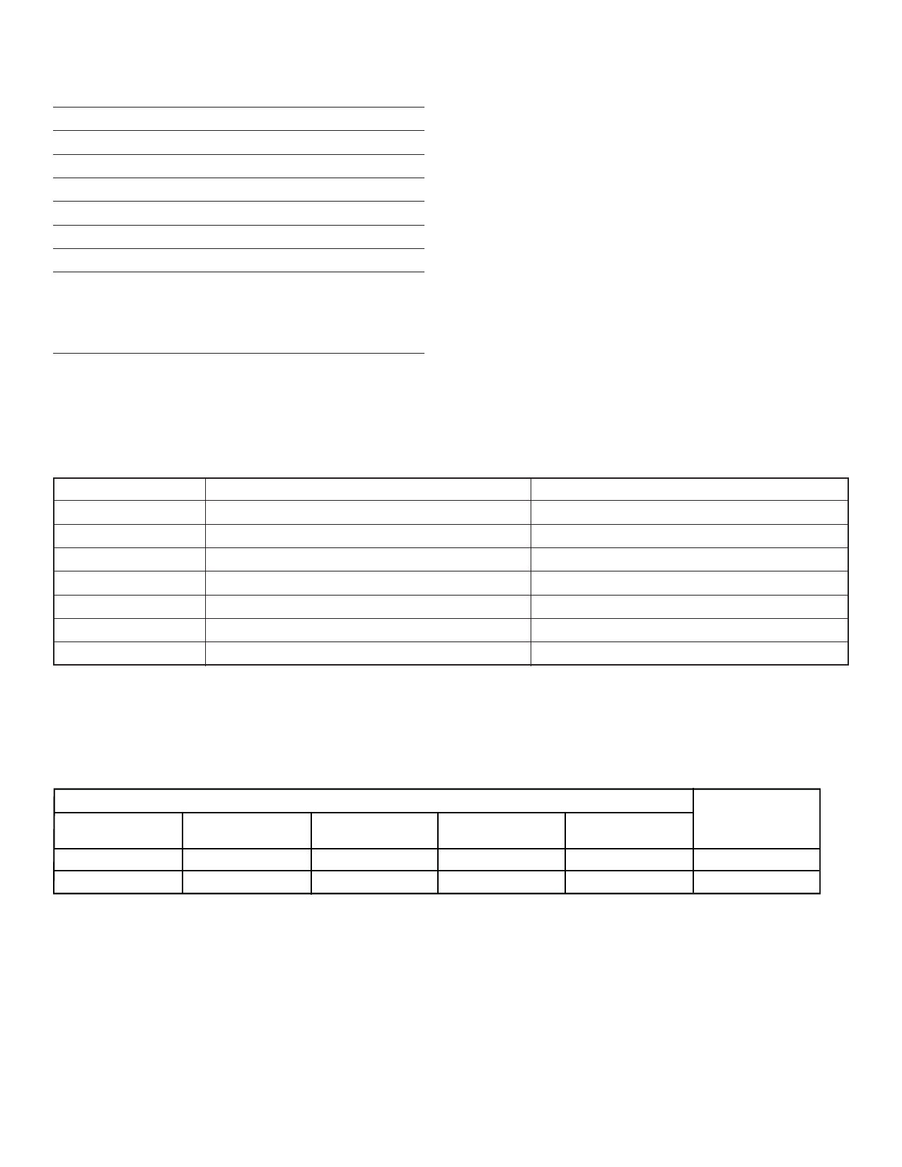
Absolute Maximum Ratings*
VDD Logic power supply voltage
VPP - VNN Supply voltage
VPP Positive high voltage supply
VNN Negative high voltage supply
Logic input voltages
Analog Signal Range
Peak analog signal current/channel
-0.5V to +15V
220V
-0.5V to VNN +200V
+0.5V to -200V
-0.5V to VDD +0.3V
V to V
NN
PP
3.0A
Storage temperature
-65°C to +150°C
Power dissipation:
28-lead PLCC
48-lead TQFP
26-lead TAPP
26-lead µ-BGA
1.2W
1.0W
1.0W
1.0W
* Absolute Maximum Ratings are those values beyond which damage
to the device may occur. Functional operation under these condi-
tions is not implied. Continuous operation of the device at the
absolute rating level may affect device reliability. All voltages are
referenced to device ground.
HV230/232
Operating Conditions*
Symbol
Parameter
Value
VDD
Logic power supply voltage1, 3
VPP
Positive high voltage supply1, 3
VNN
Negative high voltage supply1, 3
VIH
High-level input voltage
VIL
Low-level input voltage
VSIG
Analog signal voltage peak to peak
TA
Operating free air-temperature
4.5V to 13.2V
40V to VNN+ 200V
-40V to -160V
VDD -1.5V to VDD
0V to 1.5V
VNN +10V to VPP -10V2
0°C to 70°C
Notes:
1 Power up/down sequence is arbitrary except GND must be powered-up first and powered-down last.
2 VSIG must be VNN - VSIG - VPP or floating during power up/down transistion.
3 Rise and fall times of power supplies VDD, VPP, and VNN should not be less than 1.0msec.
Ordering Information
28-Lead plastic
chip carrier
HV232PJ
-
48-Lead TQFP
HV232FG
-
Package Options
26-lead TAPP
-
HV230TA
26-lead µ-BGA
HV232GA
-
Die
HV232X
-
VPP - VNN
200V
200V
2
NR032505
Share Link: 