IDT75K72100 データシートの表示(PDF) - Integrated Device Technology
部品番号
コンポーネント説明
メーカー
IDT75K72100 Datasheet PDF : 3 Pages
| |||

IP Co-Processor 256K x 72 Entries
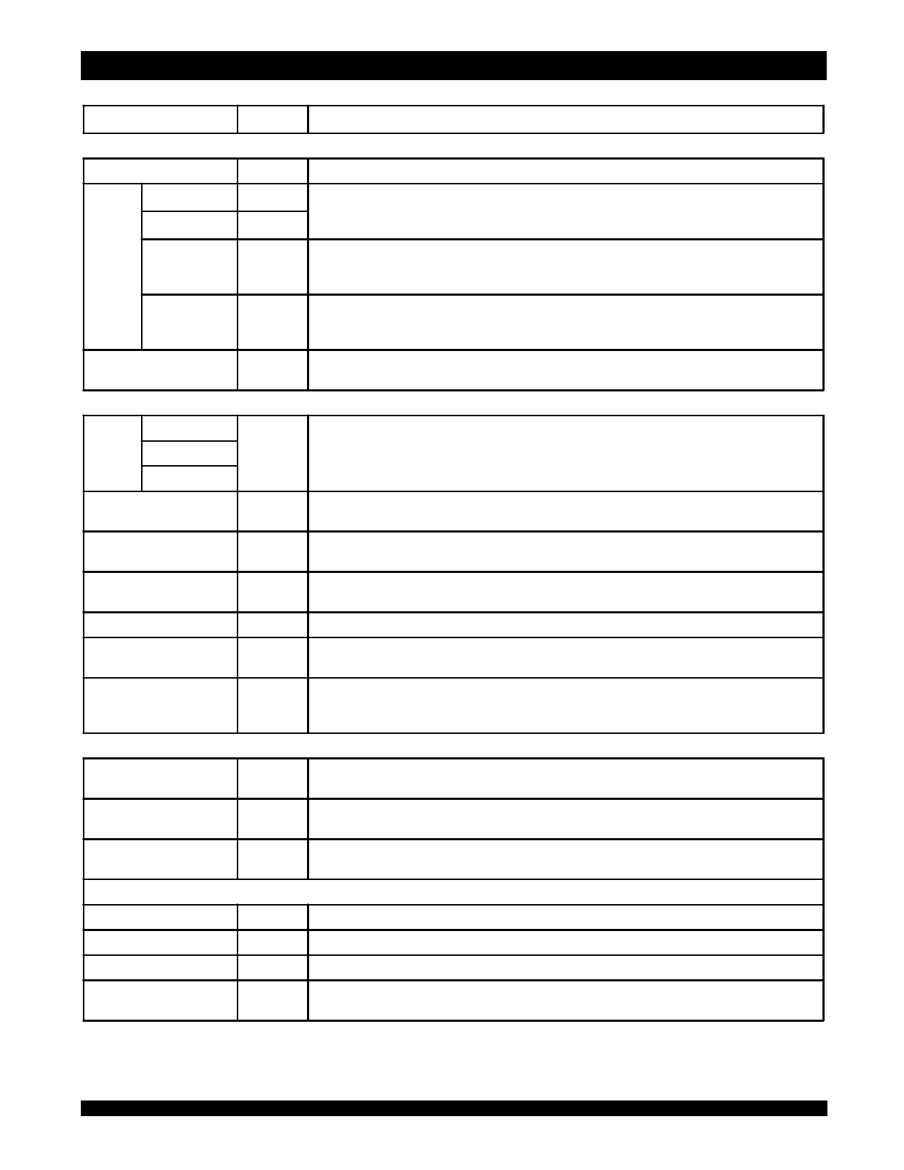
Signal Descriptions
Datasheet Brief 75K72100
Pin Function
I/O Description
NSE Request Bus:
Request Strobe
Input This input signifies a valid input request and signals the start of an NSE operation cycle.
Instruction
Lookup Type
Input These two fields of the Command bus define the instruction to be performed by the NSE and the lookup
type. The lookup type is selected only for operational type commands (Lookups, Learns) and is a "don't
Input care" for maintenance typ e commands (all Reads and Writes).
Command Global Mask
Bus Register Select
This field is within the Command bus. During Lookup or Write operations, this field defines which of the
Input Global Mask Register groups are b eing accessed. This field is a "don't care" for Read, SRAM No Wait
Read, and Learn Operations.
Comparand and
Result Register
Select
This is a multiplexed field within the Command Bus that specifies both the Result Register to store the
Input Index into, and the Comparand Reg ister to use. This field is sampled every input clock cycle. The first
cycle decodes the selected Comparand Register and the second decodes the selected Result Register.
Request Data Bus
Input/Output The Request Data Bus is a multiplexed address/data bus used to perform reads (and writes) from (to) the
Three State NSE, and to present search data for lookups.
NSE Response Bus:
Index Bus
Address
Device ID
Lookup Type
Chip Enable/ Output Enable
Write Enable
Output
Three State
This bus is used to drive the address of an external SRAM, or feedback Lookup result information
directly to the NSE's ASIC/FPGA. The Index Bus contain the encoded location at which the compare was
found, the address of the NSE which found the result and the Lookup type.
Output This signal is driven along with the Index Bus. It is connected to the CE input pin of a ZBT SRAM or to the
Three State OE pin of a PBSRAM.
Output This signal is driven along with the Index bus. It is used to assert the WE pin of an external SRAM. It is
Three State active for both SRAM write operations and the Learn command.
Read Acknowledge
Output
This signal is sent back when the data is read from the NSE on the Request Data Bus, or when the data
being read from the associated external SRAM.
Match Acknowledge
Output This is signal is sent with the Index. It will be driven low if there was no match, high if a match was found.
Valid
Lookup Bit
Output
This signal is sent with the Index. It will be driven high upon the completion of a lookup, even if the
lookup did not result in a hit.
Multi Match
Output
Output
(Open Drain)
This signal is sent with the Index. It shall go active when a) multiple hits occur in one segment; or, b) one
or more hits occur in two (or more) segments; or, c) one or more hits occur in multiple devices that are
depth cascaded.
Depth Expansion:
Device Address
Input
These three DC pins are used to define the Device Address for each of the eight possible depth
expanded NSE devices in an NSE system.
Match
Input
Input
The Match Input signal is driven by all upstream Match Output signals. This indicates to all down stream
NSEs that a hit in a higher priority NSE has occurred.
Match
Output
Output
The Match Output signal signifies that a match has occurred in the NSE. The signal is fed into a Match
Input line of all lower priority NSE(s).
Clock and Initialization:
Clock Input
Input All inputs and outputs are referenced to this clock.
Reset
Input This pin will force all outputs to a high impedence condition, as well as clearing the NSE enable bit.
Last NSE
Last SRAM
Input This pin defines which NSE device will drive the ASIC Feedback signals to the ASIC/FPGA.
Input
This pin defines which NSE device will drive the SRAM control signals CE/OE and WE. It also defaults
this device to driving the Index Bus when there is no ongoing operation preventing the bus from floating.
6074 tbl 01
6.432