LC3564RM „Éá„Éľ„āŅ„ā∑„Éľ„Éą„ĀģŤ°®Á§ļÔľąPDFÔľČ - SANYO -> Panasonic
ťÉ®ŚďĀÁē™ŚŹ∑
„ā≥„É≥„ÉĚ„Éľ„Éć„É≥„ÉąŤ™¨śėé
„É°„Éľ„āę„Éľ
LC3564RM Datasheet PDF : 10 Pages
| |||
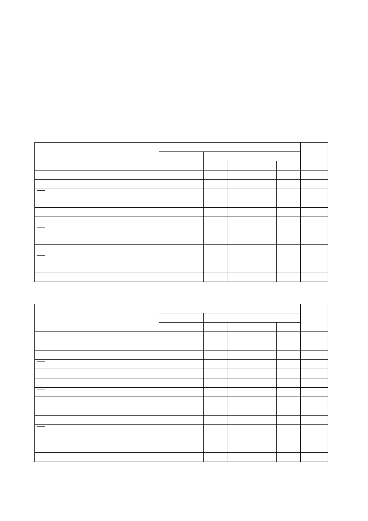
LC3564RM,RT-10LV/12LV/15LV
AC Electrical Characteristics at Ta = ‚Äď40 to +85¬įC, VCC = 2.7 to 3.6V
AC test conditions
Input pulse voltage level: 0.2VCC to 0.8 VCC
Input rise and fall times: 5 ns
Input/output timing level: VCC/2
Output load: 30 pF (including jig capacitance)
Read Cycle
Parameter
Read cycle time
Address access time
CE1 access time
CE2 access time
OE access time
Output hold time
CE1 output enable time
CE2 output enable time
OE output enable time
CE1 output disable time
CE2 output disable time
OE output disable time
Write Cycle
LC3564RM,RT
Symbol
-10LV
-12LV
-15LV
Unit
min.
max.
min.
max.
min.
max.
tRC
100
-
120
-
150
-
ns
tAA
-
100
-
120
-
150
ns
tCA1
-
100
-
120
-
150
ns
tCA2
-
100
-
120
-
150
ns
tOA
-
50
-
60
-
75
ns
tOH
10
-
10
-
10
-
ns
tCOE1
10
-
10
-
10
-
ns
tCOE2
10
-
10
-
10
-
ns
tOOE
5
-
5
-
5
-
ns
tCOD1
-
35
-
40
-
50
ns
tCOD2
-
35
-
40
-
50
ns
tOOD
-
25
-
30
-
40
ns
Parameter
Write cycle time
Address setup time
Write pulsewidth
CE1 setup time
CE2 setup time
Write recovery time
CE1 write recovery time
CE2 write recovery time
Data setup time
Data hold time
CE1 data hold time
CE2 data hold time
WE output enable time
WE output disable time
LC3564RM,RT
Symbol
-10LV
-12LV
-15LV
Unit
min.
max.
min.
max.
min.
max.
tWC
100
-
120
-
150
-
ns
tAS
0
-
0
-
0
-
ns
tWP
60
-
70
-
80
-
ns
tCW1
70
-
80
-
90
-
ns
tCW2
70
-
80
-
90
-
ns
tWR
0
-
0
-
0
-
ns
tWR1
0
-
0
-
0
-
ns
tWR2
0
-
0
-
0
-
ns
tDS
50
-
55
-
60
-
ns
tDH
0
-
0
-
0
-
ns
tDH1
0
-
0
-
0
-
ns
tDH2
0
-
0
-
0
-
ns
tWOE
5
-
5
-
5
-
ns
tWOD
-
35
-
40
-
45
ns
No. 4484‚ÄĒ5/10
Share Link: 