LX2202(2005) データシートの表示(PDF) - Microsemi Corporation
部品番号
コンポーネント説明
メーカー
LX2202 Datasheet PDF : 12 Pages
| |||
LX2202
TM
® 2A Li-Ion Linear Charger and Power Control
PRODUCTION DATA SHEET
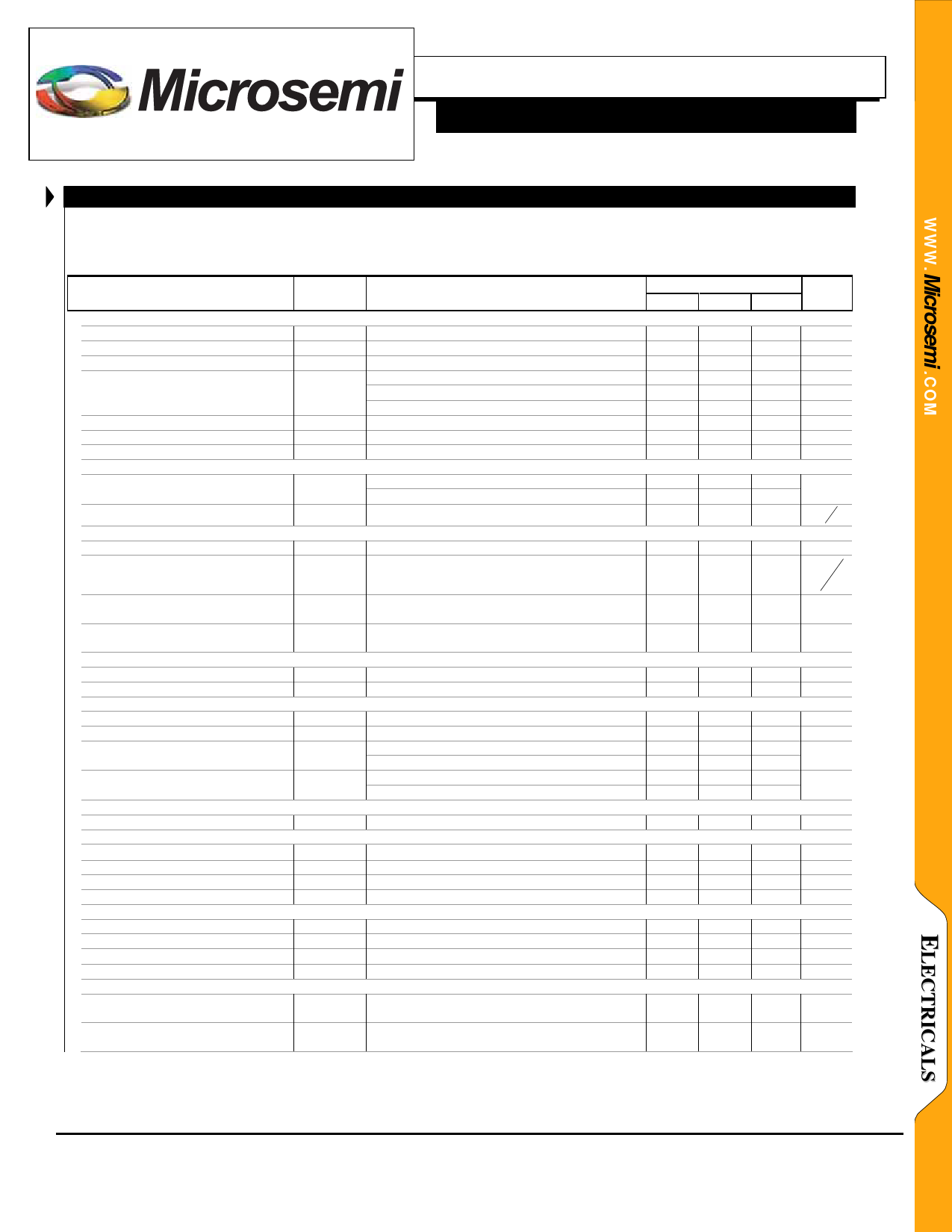
ELECTRICAL CHARACTERISTICS
Unless otherwise specified, the following specifications apply over the ambient temperature 0°C ≤ TA ≤ 70°C except where otherwise
noted and the following test conditions: VDD = 5.0V, VM = GND, VID0 = VID1 = VBAT, RCCP = 72.3k, RCTP = 105k, RUSB =
2.55k.
Parameter
Symbol
Test Conditions
` MAIN CIRCUITRY
Input Voltage
USB Input voltage
Under Voltage Charging Lockout
Quiescent Current
CTP Bias Voltage
CCP Bias Voltage
CUS Bias Voltage
` CONSTANT VOLTAGE MODE
Constant Voltage Charge Voltage
Top Off Charge Droop Threshold
` CONSTANT CURRENT MODE
BAT Constant Current Accuracy
VDD
VUSB
VDDUVLO
IGND
VCTP
VCCP
VCUS
VBAT = 0; Rising VDD
VDD > VBAT
VDD < VBAT
VDD < VBAT, VID0 = VID1 = 0V
IBAT > 100mA
VCVL
VDRP
VM = Lo; -40C to 125C
VM = Hi; -40 to 125C
ICCL
Conditioning Current
ICOND
VBAT < VCTV ; @25°C
Conditioning Current Mode
Threshold Voltage
VCTV
Charge Termination Current
Accuracy
` USB CURRENT LIMIT
IBAT
@25°C
USB Low Current Limit
USB High Current Limit
` LOGIC
IIN
VUSB = 5V, VDD < VUSB, VID1 = Lo
IIN
VUSB = 5V, VDD < VUSB, VID1 = Hi
STAT Logic High Output
STAT Logic Low Output
State Select Threshold
VSTAT
VSTAT
VVID
VUSB = 5.0V, ISTAT = -5mA
VUSB = 5.0V, ISTAT = 25µA
Logic Hi
Logic Lo
VM Select Threshold
` THERMAL SHUTDOWN
VVM
Logic Hi
Logic Lo
Maximum Junction Temperature
TJ
VUSB = 5.0V, IOUT = 1A, Temperature Rising
` BI-DIRECTIONAL PASS ELEMENT CONTROL
Discharge Switch On Resistance
Charging Threshold
Discharging Threshold
Pass Element Switch Mode Delay
` PSW FET DRIVER
RDS(ON)
VCHG
VDCH
tsw
IBAT = -1A (Not Tested)
VUSB > VBAT + VCHG
VUSB < VBAT + VDCH
Charge–to–discharge or Discharge–to–charge
High Output Voltage
Low Output Voltage
VPSW
VPSW
VUSB < VBAT, IPSW = 0, VBAT = 4.2V
VUSB > VBAT, IPSW = 0
ORing Resistance
Switch Delay (after tsw)
` HEAD ROOM
RPSW
tPSW
CPSW = 1000pF, to VPSW = (VBAT – 1V)
Charging headroom
VDD – VBAT, IBATT = 5mA; not tested in
production
Discharging headroom
VBAT – VDD, IBATT = -20mA; not tested in
production
LX2202
Units
Min Typ Max
4.5
6
V
4.35
6
V
3.60 3.85
V
2.1
4
mA
20
40
µA
9
15
µA
1.26
V
1.26
V
2.6
V
4.16
4.06
4.2 4.24
4.1 4.14
V
96
97
98
% VBAT VCVL
0.85
1
1.15
A
3.0
4.6
6.0 % IBAT
ICCL
2.8
V
35
50
65
mA
85
93
100 mA
425
463
500
mA
4.5
5
V
0.4
V
2.0
0.8
V
2.0
0.8
V
130
140 150
°C
130 150 m Ω
40
mV
60
mV
5
10
µs
4.1
4.2
V
0
0.2
V
5
10
15
KΩ
0
500 1000 Ns
65
mV
65
mV
Copyright © 2004
Rev. 1.0, 2005-03-18
Microsemi
Integrated Products Division
11861 Western Avenue, Garden Grove, CA. 92841, 714-898-8121, Fax: 714-893-2570
Page 3
Share Link: 